Case Study: Rambus Memory
There was a time when computer technology would be pushed from the laboratory into the marketplace. As the consumer marketplace for computing devices exploded, the “technology push” was replaced by “market pull,” and consumer demand then dominated the preferences of technologists when it came to developing a new memory technology. High performance, expensive memory for high-end processors was displaced by high density, low-cost memory for consumer electronics, such as videogames. It became more profitable for memory manufacturers to address the needs of high volume consumer markets, rather than devote costly chip fabrication facilities to a comparatively small high-end market.
The consumer electronics industry now dominates the memory market, and even high-end, non-consumer processors make heavy use of consumer electronics technology, exploiting architectural enhancements instead, or innovations in supporting technologies (such as high speed interconnects) to compensate for the performance shortcomings of what we might call “videogame memory.”
Videogame memory is not all that low-end, however, and in fact, makes use of extraordinary technology enhancements that squeeze the most performance out of ever denser, low-cost devices. A leading memory technology that is being introduced into Intel-based personal computers in 1999 was developed by Ram- bus, Inc. The Rambus DRAM (RDRAM) retrieves a block of 8 bytes internal to the DRAM chip on every access, and multiplexes the 8 bytes onto a narrow 8-bit or 16-bit channel, operating at a rate of 800 MHz (or higher).
A typical DRAM core (that is, the storage portion of an ordinary DRAM) can store or retrieve a line of 8 bytes with a 100 MHz cycle. This is internal to the DRAM chip: most DRAMs only deliver one byte per cycle, but the RDRAM technology can multiplex that up to 1 byte per cycle using a higher external clock of 800 MHz. That higher rate is fed to a memory controller (the “chipset” on an Intel machine) which demuxes it to a 32-bit wide data stream at a lower rate, such as 200 MHz, going into a Pentium (or other processor chip).
The Rambus “RIMM” modules (Rambus Inline Memory Modules) look similar to ordinary SIMMs and DIMMs, but they operate differently. The Rambus memory uses microstrip technology (also known as transmission lines) on the motherboard, which implements a crude shield that reduces radio frequency (RF) effects that interfere with data traveling through wires on the motherboard, which are called board traces. In designing a printed circuit board (PCB) for
Rambus technology, the critical parameters are (1) dielectric thickness of the PCB, (2) separation of the memory modules, and (3) trace width. There must be a ground plane (an electrical return path) beneath every signal line, with no vias (connections between board layers) along the path. All signals go on the top layer of the PCB. (A PCB can have a number of layers, typically no more than 8). The memory controller and memory modules must all be equally spaced, such as
.5 inches from the memory controller to the first RIMM, then .5 in to the next, etc.
The “Rambus Channel” is made up of transmission line traces. The trace widths end up being about twice as wide as ordinary traces, on the order of 12 mils (300 microns). Although 300 microns is relatively small for a board trace, if we want to send 128 signals over a PCB, using a 600 micron pitch (center-to-center spacing) with 300 microns between 300 micron traces, this corresponds to a foot- print of 128 ´ 600 microns = 76 mm. This is a large footprint compared with lower speed solutions that allow a much closer packing density.
In reality, the Rambus Channel only has 13 high speed signals, (the address is serialized onto a single line, there are 8 data lines, 1 parity line, 2 clock lines, and 1 command line) and so the seemingly large footprint is not a near-term problem. With a 16-bit version of the Rambus Channel on the horizon, the band- width problem appears to be in hand for a number of years using this technology. Extensibility to large word widths such as 64 bits or 128 bits will pose a significant challenge down the road, however, because the chipset will need to support that same word width – a formidable task with current packaging methods, that already have over 500 pins on the chipset.
Although Rambus memory of this type became available in 1998, the RIMM modules were not widely available until 1999, timed for the availability of a new memory controller (chipset) for the RIMMs. The memory controller is an important aspect of this type of memory because the view of memory that the CPU perceives is different from the physical memory.
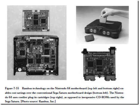
Rambus memory is more expensive than conventional DRAM memory, but overall system cost can be reduced, which makes it attractive in low-cost, high performance consumer electronics such as the Nintendo 64 video game console. The Nintendo 64 (see Figure 7-35) has four primary chips: a 64-bit MIPS RS4300i CPU; a Reality coprocessor which integrates all graphics, audio and memory management functions; and two Rambus memory chips.
The Rambus technology provides the Nintendo 64 with a bandwidth of 562.5 MB/s using a 31-pin interface to the memory controller. By comparison, a sys- tem using typical 64-bit-wide synchronous DRAMs (SDRAMs) requires a 110-pin interface to the memory controller. This reduction in pin count allows the memory controller to fit on the same die (the silicon chip) as the graphics and sound functions, in a relatively low-cost, 160-pin packaged chip.
The Rambus memory subsystem is made up of two memory chips which occupy 1.5 square inches of board space. An equivalent SDRAM design would require 6 square inches of board space. The space savings of using the Rambus approach enabled Nintendo to fit all of its components on a board measuring five by six inches, which is one quarter the size of the system board used in the competing Sega Saturn. In addition, Nintendo was able to use only a two-layer board instead of the four layers used in the Sega Saturn.
The cost savings Nintendo realized by choosing the Rambus solution over the 64-bit SDRAM approach are considerable, but should be placed in perspective with the overall market. The ability to use a two-layer implementation saved Nintendo $5 per unit in manufacturing costs. Taken altogether, Nintendo estimates the total bill of materials cost savings over an equivalent SDRAM-based design was about 20 percent.
These cost savings need to be placed in perspective with the marketplace, how- ever. The competing Sega Saturn and Sony Playstation use CD-ROMs for game storage, which cost under $2 each to mass produce. The Nintendo 64 uses a plug-in ROM cartridge that costs closer to $10 each to mass produce, and can only store 1% of what can be stored on a CD-ROM. This choice of media may have a great impact on the overall system architecture, and so the Rambus approach may not benefit all systems to the same degree. Details matter a great deal when it comes to evaluating the impact of a new technology on a particular market, or even a segment of a market.
Case Study: The Intel Pentium Memory System
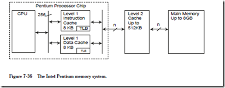
The Intel Pentium processor is typical of modern processors in its memory con- figurations. Figure 7-36 shows a simplified diagram of the memory elements and
data paths. There are two L1 caches on board the actual Pentium chip, an instruction, or I-cache, and a data, or D-cache. Each cache has a 256 bit (32 byte) line size, with an equally-sized data path to the CPU. The L1 caches are 2-way set associative, and each way has a single LRU bit. The D-cache can be set to write-through or writeback on a per-line basis. The D cache is write no-allocate: misses on writes do not result in a cache fill. Each cache is also equipped with a TLB that translates virtual to physical addresses. The D-cache TLB is 4-way set associative, with 64 entries, and is dual-ported, allowing two simultaneous data reference translations. The I-cache TLB is 4-way set associative with 32 entries.
The L2 cache, if present, is 2-way set associative, and can be 256 KB or 512 KB in size. The data bus, shown as “n” in the figure, can be 32, 64, or 128 bits in size.
THE MESI PROTOCOL
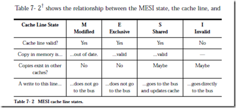
The Pentium D cache, and the L2 cache if present support the MESI cache coherency protocol for managing multiprocessor access to memory. Each D-cache line has two bits associated with it that store the MESI state. Each cache line will be in one of the four states:
• M – Modified. The contents of the cache line have been modified and are different from main memory.
• E – Exclusive. The contents of the cache line have not been modified, and are the same as the line in main memory.
• S – Shared. The line is, or may be shared with another cache line belonging to another processor.
• I – Invalid. The line is not in the cache. Reads to lines in the I state will result in cache misses.
the equivalent line in main memory. The MESI protocol is becoming a standard way of dealing with cache coherency in multiprocessor systems.
The Pentium processor also supports up to six main memory segments (there can be several thousand segments, but no more than 6 can be referenced through the segment registers.) As discussed in the chapter, each segment is a separate address space. Each segment has a base—a starting location within the 32-bit physical address space, and a limit, the maximum size of the segment. The limit may be either 216 bytes or 216 ´ 212 bytes in size. That is, the granularity of the limit may be one byte or 212 bytes in size.
Paging and segmentation on the Pentium can be applied in any combination:
Unsegmented, unpaged memory: The virtual address space is the same as the physical address space. No page tables or mapping hardware is needed. This is good for high performance applications that do not have a lot of complexity, that do not need to support growing tables, for example.
Unsegmented, paged memory: Same as for the unsegmented, unpaged memory above, except that the linear address space is larger as a result of using disk storage. A page table is needed to translate between virtual and physical addresses. A translation lookaside buffer is needed on the Pentium core, working in conjunction with the L1 cache, to reduce the number of page table accesses.
Segmented, unpaged memory: Good for high complexity applications that need to support growing data structures. This is also fast: segments are fewer in number than pages in a virtual memory, and all of the segmentation mapping hardware typically fits on the CPU chip. There is no need for disk accesses as there would be for paging, and so access times are more predictable than when paging is used.
Segmented, paged memory: A page table, segment mapping registers, and TLB all work in conjunction to support multiple address spaces.
Segmentation on the Intel Pentium processor is quite powerful but is also quite complex. We only explore the basics here, and the interested reader is referred to (Intel, 1993) for a more complete description.


