Advanced Topics
This section covers two topics that are of practical importance in designing memory systems: tree decoders and content-addressable memories. The former are required in large memories. The latter are required for associative caches, such as a TLB, or in other situations when data must be looked up at high speed based on its value, rather than on the address of where it is stored.
TREE DECODERS
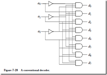
Decoders (see Appendix A) do not scale well to large sizes due to practical limitations on fan-in and fan-out. The decoder circuit shown in Figure 7-28 illustrates
the problem. For N address bits, every AND gate has a fan-in of N. Each address line is fanned out to 2N AND gates. The circuit depth is two gates.
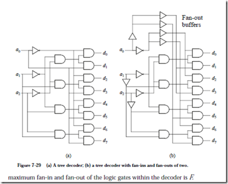
The circuit shown in Figure 7-29a is a tree decoder, which reduces the fan-in and fan-out by increasing circuit depth. For this case, each AND gate has a fan-in of F (for this example, F = 2) and only the address line that is introduced at the deepest level (a0 here) is fanned out to 2N/2 AND gates. The depth has now increased to logF(2N). The large fan-out for the higher order address bits may be a problem, but this can be easily fixed without increasing the circuit depth by adding fan-out buffers in the earlier levels, as shown in Figure 7-29b.
Thus, the depth of a memory decoder tree is logF(2N), the width is 2N, and the
DECODERS FOR LARGE RAMS
For very large RAMs, if the 2-1/2D decoding scheme is not used, tree decoders are employed to keep fanin and fanout to manageable levels. In a conventional RAM an M-bit wide address uniquely identifies one memory location out of a memory space of 2M locations. In order to access a particular location, an address is presented to the root of a decoder tree containing M levels and 2M leaves. Starting with the root (the top level of the tree) a decision is made at each ith level of the tree, corresponding to the ith bit of the address. If the ith bit is 0 at the ith level, then the tree is traversed to the left, otherwise the tree is traversed to the right. The target leaf is at level M – 1 (counting starts at 0). There is exactly one leaf for each memory address.
The tree structure results in an access time that is logarithmic in the size of the memory. That is, if a RAM contains N words, then the memory can be accessed in OélogFNù time, where F is the fan-out of the logic gates in the decoder tree (here, we assume a fan-out of two). For a RAM of size N, M = élogFNù address bits are needed to uniquely identify each word. As the number of words in the memory grows, the length of the address grows logarithmically, so that one level of depth is added to the decoder tree each time the size of the memory doubles. As a practical example, consider a 128 megaword memory that requires 27 levels of decoding (227 = 128 Mwords). If we assume that logic gates in the decoding tree switch in 2 ns, then an address can be decoded in 54 ns.
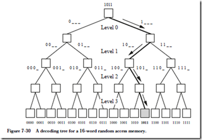
A four level decoder tree for a 16-word RAM is shown in Figure 7-30. As an
example of how the decoder tree works, the address 1011 is presented at the root node. The most significant bit in the address is a 1 so the right path is traversed at Level 0 as indicated by the arrow. The next most significant bit is a 0 so the left path is traversed at Level 1, the next bit is a 1 so the right path is traversed at Level 2, and the least significant bit is a 1 so the rightmost path is traversed next and the addressed leaf is then reached at Level 3.
CONTENT-ADDRESSABLE (ASSOCIATIVE) MEMORIES
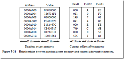
In an ordinary RAM, an address is applied to the memory, and the contents of the given location are either read or written. In a content-addressable memory (CAM), also known as an associative memory, a word composed of fields is applied to the memory and the resulting address (or index) is returned if the word or field is present in the memory. The physical location of a CAM word is generally not as significant as the values contained in the fields of the word. Relationships between addresses, values, and fields for RAM and CAM are shown in Figure 7-31.
Values are stored in sequential locations in a RAM, with an address acting as the key to locate a word. Four-byte address increments are used in this example, in which the word size is four bytes. Values are stored in fields in the CAM, and in principle any field of a word can be used to key on the rest of the word. If the CAM words are reordered, then the contents of the CAM are virtually unchanged since physical location has no bearing on the interpretation of the fields. A reordering of the RAM may change the meanings of its values entirely. This comparison suggests that CAM may be a preferred means for storing information when there is a significant cost in maintaining data in sorted order.
When a search is made through a RAM for a particular value, the entire memory may need to be searched, one word at a time, when the memory is not sorted. When the RAM is maintained in sorted order, a number of accesses may still be required to either find the value being searched or to determine the value is not stored in the memory. In a CAM, the value being searched is broadcast to all of the words simultaneously, and logic at each word makes a field comparison for membership, and in just a few steps the answer is known. A few additional steps may be needed to collect the results but in general the time required to search a CAM is less than for a RAM in the same technology, for a number of applications.
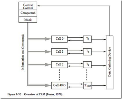
Except for maintaining tags in cache memories and in translating among net- work addresses for routing applications (see Chapter 8), CAMs are not in common use largely due to the difficulty of implementing an efficient design with conventional technology. Consider the block diagram of a CAM shown in Figure
7-32. A Central Control unit sends a comparand to each of 4096 cells, where
comparisons are made. The result is put in the Tag bits Ti which are collected by a Data Gathering Device and sent to the Central Control unit (Note that “Tag” is used differently here than in cache memory). When the Central Control unit loads the value to be searched into the comparand register, it sets up a mask to block out fields that are not part of the value. A small local processor in each cell makes a comparison between its local word and the broadcast value and reports the result of the comparison to the Data Gathering Device.
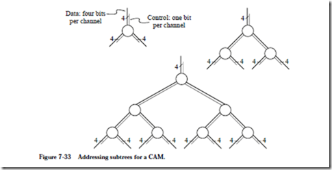
A number of problems arise when an attempt is made to implement this CAM architecture in a conventional technology such as very large scale integration (VLSI). The broadcast function that sends the comparand to the cells can be implemented with low latency if a tree structure is used. An H-tree (Mead and Conway, 1980) can be used for the tree layout if it will fit on a single IC. If the tree cannot be contained on a single chip, then connections must be made among a number of chips, which quickly limits chip density. For example, a node of a tree that has a single four-bit input and two four-bit outputs needs 12 input/output (I/O) pins and three control pins if only one node is placed on a chip. A three node subtree needs 25 pins and a seven node subtree needs 45 pins
as illustrated in Figure 7-33. A 63 node subtree requires 325 pins, excluding
power and control pins, which is getting close to the limit of most present day packaging technologies which do not go much higher than 1000 pins per pack- age. A useful CAM would contain thousands of such nodes with wider data paths, so the I/O bandwidth limit is realized early in the design of the CAM. Compromises can be made by multiplexing data onto the limited number of I/O connections but this reduces effective speed, which is a major reason for using a CAM in the first place.
Although implementations of CAMs are difficult, they do find practical uses, such as in TLBs and in computer networks. One application is in a network controller which receives data packets from several processors and then distributes those packets back to the processors or to other network controllers. Each processor has a unique address which the CAM keys on to determine if the target processor for a packet is in its own network or if it must be forwarded to another network.
MEMORY DESIGN EXAMPLE: A DUAL-PORT RAM
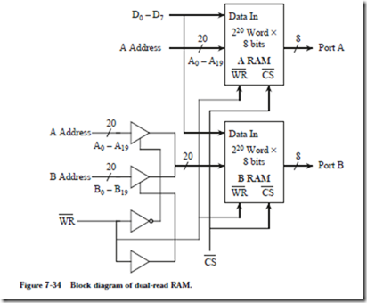
A dual-read, or dual-port RAM allows any two words to be simultaneously read from the same memory. As an example, we will design a 220 word by 8-bit dual-read RAM. For our design, any two words can be read at a time, but only one word can be written at a time. Our approach is to create two separate 220 word memories. When writing into the dual-read RAM, the address lines of both
single-read RAMs are set identically and the same data is written to both single-read memories. During a read operation, the address lines of each single-read RAM are set independently, so that two different words can be simultaneously read.
Figure 7-34 shows a block diagram for the dual-read RAM. During a write oper-
ation, the A address is used for both single-read RAMs. Tri-state buffers at the B RAM address inputs are controlled by the WR line. When WR=0, the A address is used at the B address input, otherwise, the B address is used at the B address input. The numbers that appear adjacent to the slashes indicate the number of individual lines that are represented by the single line. An 8 next to a slash indicates 8 lines, and a 20 next to a slash indicates 20 lines.
Each tri-state buffer has 20 input lines and 20 output lines, but Figure 7-34 uses a notation in which a single buffer represents 20 separate tri-state buffers that share the same control input. A buffer delay is inserted on the WR line in order to compensate for the delay on the complemented WR line, so that the A and B addresses are not unintentionally simultaneously enabled.
