INPUT AND OUTPUT
In the earlier chapters, we considered how the CPU interacts with data that is accessed internal to the CPU, or is accessed within the main memory, which may be extended to a hard magnetic disk through virtual memory. While the access speeds at the different levels of the memory hierarchy vary dramatically, for the most part, the CPU sees the same response rate from one access to the next. The situation when accessing input/output (I/O) devices is very different.
• The speeds of I/O data transfers can range from extremely slow, such as reading data entered from a keyboard, to so fast that the CPU may not be able to keep up, as may be the case with data streaming from a fast disk drive, or real time graphics being written to a video monitor.
• I/O activities are asynchronous, that is, not synchronized to the CPU clock, as are memory data transfers. Additional signals, called handshaking signals, may need to be incorporated on a separate I/O bus to coordinate when the device is ready to have data read from it or written to it.
• The quality of the data may be suspect. For example, line noise during data transfers using the public switched telephone network, or errors caused by media defects on disk drives mean that error detection and correction strategies may be needed to ensure data integrity.
• Many I/O devices are mechanical, and are in general more prone to failure than the CPU and main memory. A data transfer may be interrupted due to mechanical failure, or special conditions such as a printer being out of paper, for example.
• I/O software modules, referred to as device drivers, must be written in such a way as to address the issues mentioned above.
In this chapter we discuss the nature of communicating using busses, starting
first with simple bus fundamentals and then exploring multiple-bus architectures. We then take a look at some of the more common I/O devices that are connected to these busses.
In the next sections we discuss communications from the viewpoints of communications at the CPU and motherboard level, and then branch out to the local area network.
8.1 Simple Bus Architectures
A computer system may contain many components that need to communicate with each other. In a worst case scenario, all N components need to simultaneously communicate with every other component, in which N2/2 links are needed for N components. The number of links becomes prohibitively large for even small values of N, but fortunately, as for long distance telecommunication, not all devices need to simultaneously communicate.
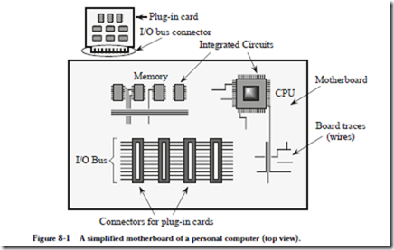
A bus is a common pathway that connects a number of devices. An example of a bus can be found on the motherboard (the main circuit board that contains the central processing unit) of a personal computer, as illustrated in simplified form in Figure 8-1. (For a look at a real motherboard, see Figure 1-6.) A typical moth-
erboard contains integrated circuits (ICs) such as the CPU chip and memory
chips, board traces (wires) that connect the chips, and a number of busses for chips or devices that need to communicate with each other. In Figure 8-1, an I/O bus is used for a number of cards that plug into the connectors, perpendicular to the motherboard in this example configuration.
8.1.1 BUS STRUCTURE, PROTOCOL, AND CONTROL
A bus consists of the physical parts, like connectors and wires, and a bus proto- col. The wires can be partitioned into separate groups for control, address, data, and power as illustrated in Figure 8-2. A single bus may have a few different
power lines, and the example shown in Figure 8-2 has lines for ground (GND) at 0 V, and positive and negative voltages at +5 V, and –15 V, respectively.
The devices share a common set of wires, and only one device may send data at any one time. All devices simultaneously listen, but normally only one device receives. Only one device can be a bus master, and the remaining devices are then considered to be slaves. The master controls the bus, and can be either a sender or a receiver.
An advantage of using a bus is to eliminate the need for connecting every device with every other device, which avoids the wiring complexity that would quickly dominate the cost of such a system. Disadvantages of using a bus include the slowdown introduced by the master/slave configuration, the time involved in implementing a protocol (see below), and the lack of scalability to large sizes due to fan-out and timing constraints.
A bus can be classified as one of two types: synchronous or asynchronous. For a synchronous bus, one of the devices that is connected to the bus contains an oscillator (a clock) that sends out a sequence of 1’s and 0’s at timed intervals as illustrated in Figure 8-3. The illustration shows a train of pulses that repeat at 10 ns intervals, which corresponds to a clock rate of 100 MHz. Ideally, the clock
would be a perfect square wave (instantaneous rise and fall times) as shown in the figure. In practice, the rise and fall times are approximated by a rounded, trapezoidal shape.
8.1.2 BUS CLOCKING
For a synchronous bus, discussed below, a clock signal is used to synchronize bus operations. This bus clock is generally derived from the master system clock, but it may be slower than the master clock, especially in higher-speed CPUs. For example, one model of the Power Macintosh G3 computer has a system clock speed of 333 MHz, but a bus clock speed of 66 MHz, which is slower by a factor of 5. This corresponds with memory access times which are much longer than internal CPU clock speeds. Typical cache memory has an access time of around 20 ns, compared to a 3 ns clock period for the processor described above.
In addition to the bus clock running at a slower speed than the processor, several bus clock cycles are usually required to effect a bus transaction, referred to collectively as a single bus cycle. Typical bus cycles run from two to five bus clock periods in duration.
8.1.3 THE SYNCHRONOUS BUS
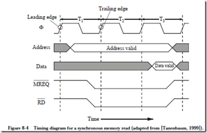
As an example of how communication takes place over a synchronous bus, con- sider the timing diagram shown in Figure 8-4 which is for a synchronous read of a word of memory by a CPU. At some point early in time interval T1, while the clock is high, the CPU places the address of the location it wants to read onto the address lines of the bus. At some later time during T1, after the voltages on the address lines have become stable, or “settled,” the ![]() and RD lines are asserted by the CPU.
and RD lines are asserted by the CPU.
![]() informs the memory that it is selected for the transfer (as opposed to another device, like a disk). The RD line informs the selected device to perform a read operation. The overbars on
informs the memory that it is selected for the transfer (as opposed to another device, like a disk). The RD line informs the selected device to perform a read operation. The overbars on![]() and RD indicate that a 0 must be placed on these lines in order to assert them.
and RD indicate that a 0 must be placed on these lines in order to assert them.
The read time of memory is typically slower than the bus speed, and so all of time interval T2 is spent performing the read, as well as part of T3. The CPU assumes a fixed read time of three bus clocks, and so the data is taken from the bus by the CPU during the third cycle. The CPU then releases the bus by de-asserting MREQ and RD in T3. The shaded areas of the data and address portions of the timing diagram indicate that these signals are either invalid or unimportant at those times. The open areas, such as for the data lines during T3, indicate valid signals. Open and shaded areas are used with crossed lines at either end to indicate that the levels of the individual lines may be different.
8.1.4 THE ASYNCHRONOUS BUS
If we replace the memory on a synchronous bus with a faster memory, then the memory access time will not improve because the bus clock is unchanged. If we increase the speed of the bus clock to match the faster speed of the memory, then slower devices that use the bus clock may not work properly.
An asynchronous bus solves this problem, but is more complex, because there is no bus clock. A master on an asynchronous bus puts everything that it needs on the bus (address, data, control), and then asserts MSYN (master synchronization). The slave then performs its job as quickly as it can, and then asserts SSYN (slave synchronization) when it is finished. The master then de-asserts MSYN , which signals the slave to de-assert SSYN . In this way, a fast master/slave combination responds more quickly than a slow master/slave combination.
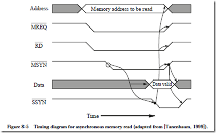
As an example of how communication takes place over an asynchronous bus, consider the timing diagram shown in Figure 8-5. In order for a CPU to read a
word from memory, it places an address on the bus, followed by asserting MREQ and RD . After these lines settle, the CPU asserts MSYN . This event triggers the memory to perform a read operation, which results in SSYN eventually being asserted by the memory. This is indicated by the cause-and-effect arrow between MSYN and SSYN shown in Figure 8-5. This method of synchronization is referred to as a “full handshake.” In this particular implementation of a full handshake, asserting MSYN initiates the transfer, followed by the slave asserting SSYN , followed by the CPU de-asserting MSYN , followed by the memory de-asserting SSYN . Notice the absence of a bus clock signal.
Asynchronous busses can be more difficult to debug than synchronous busses when there is a problem, and interfaces for asynchronous busses can be more difficult to make. For these reasons, synchronous busses are very common, particularly in personal computers.
8.1.5 BUS ARBITRATION—MASTERS AND SLAVES
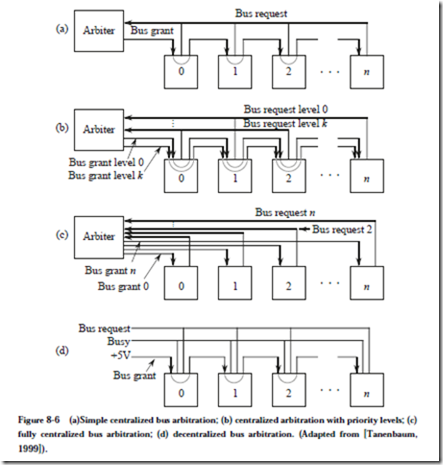
Suppose now that more than one device wants to be a bus master at the same time. How is a decision made as to who will be the bus master? This is the bus arbitration problem, and there are two basic schemes: centralized and decentralized (distributed). Figure 8-6 illustrates four organizations for these two
schemes. In Figure 8-6a, a centralized arbitration scheme is used. Devices 0 through n are all attached to the same bus (not shown), and they also share a bus request line that goes into an arbiter. When a device wants to be a bus master, it asserts the bus request line. When the arbiter sees the bus request, it determines if a bus grant can be issued (it may be the case that the current bus master will not allow itself to be interrupted). If a bus grant can be issued, then the arbiter asserts the bus grant line. The bus grant line is daisy chained from one device to the next. The first device that sees the asserted bus grant and also wants to be the bus master takes control of the bus and does not propagate the bus grant to higher
numbered devices. If a device does not want the bus, then it simply passes the bus grant to the next device. In this way, devices that are electrically closer to the arbiter have higher priorities than devices that are farther away.
Sometimes an absolute priority ordering is not appropriate, and a number of bus request/bus grant lines are used as shown in Figure 8-6(b). Lower numbered bus request lines have higher priorities than higher numbered bus request lines. In order to raise the priority of a device that is far from the arbiter, it can be assigned to a lower numbered bus request line. Priorities are assigned within a group on the same bus request level by electrical proximity to the arbiter.
Taking this to an extreme, each device can have its own bus request/bus grant line as shown in Figure 8-6(c). This fully centralized approach is the most powerful from a logical standpoint, but from a practical standpoint, it is the least scalable of all of the approaches. A significant cost is the need for additional lines (a precious commodity) on the bus.
In a fourth approach, a decentralized bus arbitration scheme is used as illustrated in Figure 8-6(d). Notice the lack of a central arbiter. A device that wants to become a bus master first asserts the bus request line, and then it checks if the bus is busy. If the busy line is not asserted, then the device sends a 0 to the next higher numbered device on the daisy chain, asserts the busy line, and de-asserts the bus request line. If the bus is busy, or if a device does not want the bus, then it simply propagates the bus grant to the next device.
Arbitration needs to be a fast operation, and for that reason, a centralized scheme will only work well for a small number of devices (up to about eight). For a large number of devices, a decentralized scheme is more appropriate.
Given a system that makes use of one of these arbitration schemes, imagine a situation in which n card slots are used, and then card m is removed, where m < n. What happens? Since each bus request line is directly connected to all devices in a group, and the bus grant line is passed through each device in a group, a bus request from a device with an index greater than m will never see an asserted bus grant line, which can result in a system crash. This can be a frustrating problem to identify, because a system can run indefinitely with no problems, until the higher numbered device is accessed.
When a card is removed, higher cards should be repositioned to fill in the missing slot, or a dummy card that continues the bus grant line should be inserted in
place of the removed card. Fast devices (like disk controllers) should be given higher priority than slow devices (like terminals), and should thus be placed close to the arbiter in a centralized scheme, or close to the beginning of the Bus grant line in a decentralized scheme. This is an imperfect solution given the opportunities for leaving gaps in the bus and getting the device ordering wrong. These days, it is more common for each device to have a separate path to the arbiter.


