8.2 Case Study: Communication on the Intel Pentium Architecture
The Intel Pentium processor family is Intel’s current state-of-the art implementation of their venerable x86 family, which began with the Intel 8086, released in 1978. The Pentium is itself a processor family, with versions that emphasize high speed, multiprocessor environments, graphics, low power, etc. In this section we examine the common features that underlie the Pentium System Bus, which connects the Pentium to the Host Bridge (see Section 8.2).
8.2.1 SYSTEM CLOCK, BUS CLOCK, AND BUS SPEEDS
Interestingly, the system clock speed is set as a multiple of the bus clock. The value of the multiple is set by the processor whenever it is reset, according to the values on several of its pins. The possible values of the multiple vary across family members. For example, the Pentium Pro, a family member adapted for multiple CPU applications, can have multipliers ranging from 2 to 3-1/2. We mention again here that the reason for clocking the system bus at a slower rate than the CPU is that CPU operations can take place faster than memory access operations. A common bus clock frequency in Pentium systems is 66 MHz.
8.2.2 ADDRESS, DATA, MEMORY, AND I/O CAPABILITIES
The system bus effectively has 32 address lines, and can thus address up to 4 GB of main memory. Its data bus is 64 bits wide; thus the processor is capable of transferring an 8-byte quadword in one bus cycle. (Intel x86 words are 16-bits long.) We say “effectively” because in fact the Pentium processor decodes the least significant three address lines, A2-A0, into eight “byte enable” lines, BE0#-BE7#, prior to placing them on the system bus.1 The values on these eight lines specify the byte, word, double word, or quad word that is to be transferred from the base address specified by A31-A3.
8.2.3 DATA WORDS HAVE SOFT-ALIGNMENT
Data values have so-called soft alignment, meaning that words, double words, and quad words should be aligned on even word, double word, and quad word boundaries for maximum efficiency, but the processor can tolerate misaligned data items. The penalty for accessing misaligned words may be two bus cycles, which are required to access both halves of the datum.2
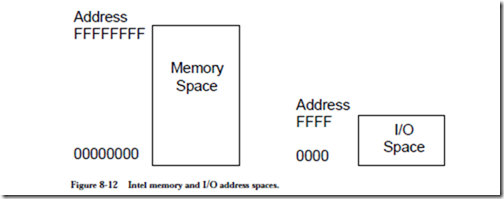
As a bow to the small address spaces of early family members, all Intel processors have separate address spaces for memory and I/O accesses. The address space to be selected is specified by the M/IO# bus line. A high value on this line selects the 4 GB memory address space, and low specifies the I/O address space. Separate opcodes, IN and OUT, are used to access this space. It is the responsibility of all devices on the bus to sample the M/IO# line at the beginning of each bus cycle to determine the address space to which the bus cycle is referring—memory or I/O. Figure 8-12 shows these address spaces graphically. I/O addresses in the x86 family are limited to 16 bits, allowing up to 64K I/O locations.
8.2.4 BUS CYCLES IN THE PENTIUM FAMILY
The Pentium processor has a total of 18 different bus cycles, to serve different
needs. These include the standard memory read and write bus cycles, the bus hold cycle, used to allow other devices to become the bus master, an interrupt acknowledge cycle, various “burst” cache access cycles, and a number of other special purpose bus cycles. In this Case Study we examine the read and write bus cycles, the “burst read” cycle, in which a burst of data can be transferred, and the bus hold/hold acknowledge cycle, which is used by devices that wish to become the bus master.
8.2.5 MEMORY READ AND WRITE BUS CYCLES
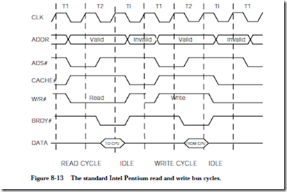
The “standard” read and write cycles are shown in Figure 8-13. By convention,
the states of the Intel bus are referred to as “T states,” where each T state is one clock cycle. There are three T states shown in the figure: T1, T2, and Ti, where Ti is the “idle” state, the state that occurs when the bus is not engaged in any specific activity, and when no requests to use the bus are pending. Recall that a “#” following a signal name indicates that a signal is active low, in keeping with Intel conventions.
Both read and write cycles require a minimum of two bus clocks, T1 and T2:
• The CPU signals the start of all new bus cycles by asserting the Address Status signal, ADS#. This signal both defines the start of a new bus cycle and signals to memory that a valid address is available on the address bus, ADDR. Note the transition of ADDR from invalid to valid as ADS# is asserted.
• The de-assertion of the cache load signal, CACHE#, indicates that the cycle will be a composed of a single read or write, as opposed to a burst read or write, covered later in this section.
• During a read cycle the CPU asserts read, W/R#, simultaneously with the assertion of ADS#. This signals the memory module that it should latch the address and read a value at that address.
• Upon a read, the memory module asserts the Burst Ready, BRDY#, signal as it places the data, DATA, on the bus, indicating that there is valid data on the data pins. The CPU uses BRDY# as a signal to latch the data values.
• Since CACHE# is deasserted, the assertion of a single BRDY# signifies the end of the bus cycle.
• In the write cycle, the memory module asserts BRDY# when it is ready to accept the data placed on the bus by the CPU. Thus BRDY# acts as a hand- shake between memory and the CPU.
• If memory is too slow to accept or drive data within the limits of two clock cycles, it can insert “wait” states by not asserting BRDY# until it is ready to respond.
8.2.6 THE BURST READ BUS CYCLE
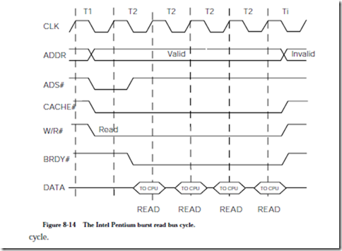
Because of the critical need to supply the CPU with instructions and data from memory that is inherently slower than the CPU, Intel designed the burst read and write cycles. These cycles read and write four eight-byte quad words in a burst, from consecutive addresses. Figure 8-14 shows the Pentium burst read
The burst read cycle is initiated by the processor placing an address on the address lines and asserting ADS# as before, but now, by asserting the CACHE# line the processor signals the beginning of a burst read cycle. In response the memory asserts BRDY# and places a sequence of four 8-byte quad words on the data bus, one quad word per clock, keeping BRDY# asserted until the entire transfer is complete.
There is an analogous cycle for burst writes. There is also a mechanism for coping with slower memory by slowing the burst transfer rate from one per clock to one per two clocks.
8.2.7 BUS HOLD FOR REQUEST BY BUS MASTER
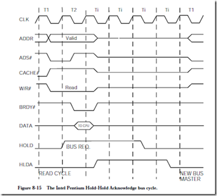
There are two bus signals for use by devices requesting to become bus master: hold (HOLD) and hold acknowledge (HLDA). Figure 8-15 shows how the transactions work. The figure assumes that the processor is in the midst of a read cycle when the HOLD request signal arrives. The processor completes the current (read) cycle, and inserts two idle cycles, Ti. During the falling edge of the
second Ti cycle the processor floats all of its lines and asserts HLDA. It keeps HLDA asserted for two clocks. At the end of the second clock cycle the device asserting HLDA “owns” the bus, and it may begin a new bus operation at the following cycle, as shown at the far right end of the figure. In systems of any complexity there will be a separate bus controller chip to mediate among the several devices that may wish to become the bus master.
8.2.8 DATA TRANSFER RATES
Let us compute the data transfer rates for the read and burst read bus cycles. In the first case, 8 bytes are transferred in two clock cycles. If the bus clock speed is 66 MHz, this is a maximum transfer rate of
or 264 million bytes per second. In burst mode this rate increases to four 8-byte bursts in five clock cycles, for a transfer rate of
or 422 million bytes per second. (Intel literature uses 4 cycles rather than 5 as the denominator, thus arriving at a burst rate of 528 million bytes per second. Take your pick.)
At the 422 million byte rate, with a bus clock multiplier of 3-1/2, the data transfer rate to the CPU is
or about 2 bytes per clock cycle. Thus under optimum, or ideal conditions, the CPU is probably just barely kept supplied with bytes. In the event of a branch instruction or other interruption in memory activity, the CPU will become starved for instructions and data.
The Intel Pentium is typical of modern processors. It has a number of specialized bus cycles that support multiprocessors, cache memory transfers, and other special situations. Refer to the Intel literature (see FURTHER READING at the end of the chapter) for more details.


