THE INSTRUCTION SET ARCHITECTURE
In this chapter we tackle a central topic in computer architecture: the language understood by the computer’s hardware, referred to as its machine language. The machine language is usually discussed in terms of its assembly language, which is functionally equivalent to the corresponding machine language except that the assembly language uses more intuitive names such as Move, Add, and Jump instead of the actual binary words of the language. (Programmers find constructs such as “Add r0, r1, r2” to be more easily understood and rendered with- out error than 0110101110101101.)
We begin by describing the Instruction Set Architecture (ISA) view of the machine and its operations. The ISA view corresponds to the Assembly Language/Machine Code level described in Figure 1-4: it is between the High Level Language view, where little or none of the machine hardware is visible or of concern, and the Control level, where machine instructions are interpreted as register transfer actions, at the Functional Unit level.
In order to describe the nature of assembly language and assembly language programming, we choose as a model architecture the ARC machine, which is a simplification of the commercial SPARC architecture common to Sun computers. (Additional architectural models are covered in The Computer Architecture Companion volume.)
We illustrate the utility of the various instruction classes with practical examples of assembly language programming, and we conclude with a Case Study of the Java bytecodes as an example of a common, portable assembly language that can be implemented using the native language of another machine.
Hardware Components of the Instruction Set Arc hitecture
The ISA of a computer presents the assembly language programmer with a view of the machine that includes all the programmer-accessible hardware, and the instructions that manipulate data within the hardware. In this section we look at the hardware components as viewed by the assembly language programmer. We begin with a discussion of the system as a whole: the CPU interacting with its internal (main) memory and performing input and output with the outside world.
THE SYSTEM BUS MODEL REVISITED
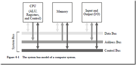
Figure 4-1 revisits the system bus model that was introduced in Chapter 1.
The purpose of the bus is to reduce the number of interconnections between the CPU and its subsystems. Rather than have separate communication paths between memory and each I/O device, the CPU is interconnected with its memory and I/O systems via a shared system bus. In more complex systems there may be separate busses between the CPU and memory and CPU and I/O.
Not all of the components are connected to the system bus in the same way. The CPU generates addresses that are placed onto the address bus, and the memory receives addresses from the address bus. The memory never generates addresses, and the CPU never receives addresses, and so there are no corresponding connections in those directions.
In a typical scenario, a user writes a high level program, which a compiler translates into assembly language. An assembler then translates the assembly language program into machine code, which is stored on a disk. Prior to execution, the machine code program is loaded from the disk into the main memory by an operating system.
During program execution, each instruction is brought into the ALU from the memory, one instruction at a time, along with any data that is needed to execute the instruction. The output of the program is placed on a device such as a video display, or a disk. All of these operations are orchestrated by a control unit, which we will explore in detail in Chapter 6. Communication among the three components (CPU, Memory, and I/O) is handled with busses.
An important consideration is that the instructions are executed inside of the ALU, even though all of the instructions and data are initially stored in the memory. This means that instructions and data must be loaded from the memory into the ALU registers, and results must be stored back to the memory from the ALU registers.
MEMORY
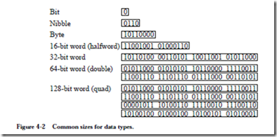
Computer memory consists of a collection of consecutively numbered (addressed) registers, each one of which normally holds one byte. A byte is a col- lection of eight bits (sometimes referred to by those in the computer communications community as an octet). Each register has an address, referred to as a memory location. A nibble, or nybble, as it is sometimes spelled, refers to a col- lection of four adjacent bits. The meanings of the terms “bit,” “byte,” and “nibble” are generally agreed upon regardless of the specifics of an architecture, but the meaning of word depends upon the particular processor. Typical word sizes are 16, 32, 64, and 128 bits, with the 32-bit word size being the common form for ordinary computers these days, and the 64-bit word growing in popularity. In this text, words will be assumed to be 32-bits wide unless otherwise specified. A comparison of these data types is shown in Figure 4-2.
In a byte-addressable machine, the smallest object that can be referenced in memory is the byte, however, there are usually instructions that read and write multi-byte words. Multi-byte words are stored as a sequence of bytes, addressed by the byte of the word that has the lowest address. Most machines today have instructions that can access bytes, half-words, words, and double-words.
When multi-byte words are used, there are two choices about the order in which the bytes are stored in memory: most significant byte at lowest address, referred
to as big-endian, or least significant byte stored at lowest address, referred to as little-endian. The term “endian” comes from the issue of whether eggs should be broken on the big or little end, which caused a war by bickering politicians in Jonathan Swift’s Gulliver’s Travels. Examples of big and little-endian formats for a 4-byte, 32-bit word is illustrated in Figure 4-3.
The bytes in a multi-byte word are stored at consecutive addresses, as shown in Figure 4-3. In a byte-addressable memory each byte is accessed by its specific address. The 4-byte word is accessed by referencing the address of the byte with the lowest address, x in Figure 4-3. This is true regardless of whether it is big-endian or little-endian. Since addresses are counted in sequence beginning with zero, the highest address is one less than the size of the memory. The highest address for a 232 byte memory is 232–1. The lowest address is 0.
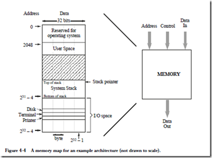
The example memory that we will use for the remainder of the chapter is shown in Figure 4-4. This memory has a 32-bit address space, which means that a pro- gram can access a byte of memory anywhere in the range from 0 to 232 – 1. The address space for our example architecture is divided into distinct regions which are used for the operating system, input and output (I/O), user programs, and
the system stack, which comprise the memory map, as shown in Figure 4-3. The memory map differs from one implementation to another, which is partly why programs compiled for the same type of processor may not be compatible across systems.
The lower 211 = 2048 addresses of the memory map are reserved for use by the operating system. The user space is where a user’s assembled program is loaded, and can grow during operation from location 2048 until it meets up with the system stack. The system stack starts at location 231 – 4 and grows toward lower addresses. The portion of the address space between 231 and 232 – 1 is reserved for I/O devices. The memory map is thus not entirely composed of real memory, and in fact there may be large gaps where neither real memory nor I/O devices exist. Since I/O devices are treated like memory locations, ordinary memory read and write commands can be used for reading and writing devices. This is referred to as memory mapped I/O.
It is important to keep the distinction clear between what is an address and what is data. An address in this example memory is 32 bits wide, and a word is also 32 bits wide, but they are not the same thing. An address is a pointer to a memory location, which holds data.
In this chapter we assume that the computer’s memory is organized in a single address space. The term address space refers to the numerical range of memory addresses to which the CPU can refer. In Chapter 7 (Memory), we will see that there are other ways that memory can be organized, but for now, we assume that memory as seen by the CPU has a single range of addresses. What decides the size of that range? It is the size of a memory address that the CPU can place on the address bus during read and write operations. A memory address that is n bits wide can specify one of 2n items. This memory could be referred to as having an n-bit address space, or equivalently as having a (2n) byte address space. For exam- ple, a machine having a 32-bit address space will have a maximum capacity of 232 (4 GB) of memory. The memory addresses will range from 0 to 232- 1, which is 0 to 4,294,967,295 decimal, or in the easier to manipulate hexadecimal for- mat, from 00000000H to FFFFFFFFFH. (The ‘H’ indicates a hexadecimal number in many assembly languages.)
THE CPU
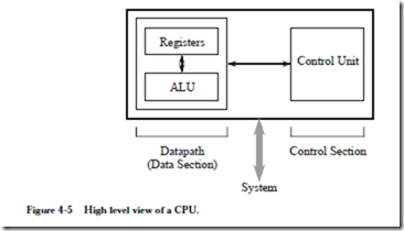
Now that we are familiar with the basic components of the system bus and memory, we are ready to explore the internals of the CPU. At a minimum, the CPU consists of a data section that contains registers and an ALU, and a control section, which interprets instructions and effects register transfers, as illustrated in Figure 4-5. The data section is also referred to as the datapath.
The control unit of a computer is responsible for executing the program instructions, which are stored in the main memory. (Here we will assume that the machine code is interpreted by the control unit one instruction at a time, though in Chapter 9 we shall see that many modern processors can process several
instructions simultaneously.) There are two registers that form the interface between the control unit and the data unit, known as the program counter (PC)† and the instruction register (IR). The PC contains the address of the instruction being executed. The instruction that is pointed to by the PC is fetched from the memory, and is stored in the IR where it is interpreted. The steps that the control unit carries out in executing a program are:
1) Fetch the next instruction to be executed from memory.
2) Decode the opcode.
3) Read operand(s) from main memory, if any.
4) Execute the instruction and store results.
5) Go to step 1.
This is known as the fetch-execute cycle.
The control unit is responsible for coordinating these different units in the execution of a computer program. It can be thought of as a form of a “computer within a computer” in the sense that it makes decisions as to how the rest of the machine behaves. We will treat the control unit in detail in Chapter 6.
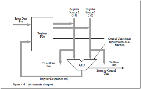
The datapath is made up of a collection of registers known as the register file and the arithmetic and logic unit (ALU), as shown in Figure 4-6. The figure depicts the datapath of an example processor we will use in the remainder of the chapter.
The register file in the figure can be thought of as a small, fast memory, separate from the system memory, which is used for temporary storage during computation. Typical sizes for a register file range from a few to a few thousand registers. Like the system memory, each register in the register file is assigned an address in sequence starting from zero. These register “addresses” are much smaller than main memory addresses: a register file containing 32 registers would have only a 5-bit address, for example. The major differences between the register file and the system memory is that the register file is contained within the CPU, and is there- fore much faster. An instruction that operates on data from the register file can often run ten times faster than the same instruction that operates on data in
memory. For this reason, register-intensive programs are faster than the equiva- lent memory intensive programs, even if it takes more register operations to do the same tasks that would require fewer operations with the operands located in memory.
Notice that there are several busses inside the datapath of Figure 4-6. Three busses connect the datapath to the system bus. This allows data to be transferred to and from main memory and the register file. Three additional busses connect the register file to the ALU. These busses allow two operands to be fetched from the register file simultaneously, which are operated on by the ALU, with the results returned to the register file.
The ALU implements a variety of binary (two-operand) and unary (one-operand) operations. Examples include add, and, not, or, and multiply. Operations and operands to be used during the operations are selected by the Control Unit. The two source operands are fetched from the register file onto busses labeled “Register Source 1 (rs1)” and “Register Source 2 (rs2).” The output from the ALU is placed on the bus labeled “Register Destination (rd),” where the results are conveyed back to the register file. In most systems these connections also include a path to the System Bus so that memory and devices can be accessed. This is shown as the three connections labeled “From Data Bus”, “To Data Bus”, and “To Address Bus.”
The Instruction Set
The instruction set is the collection of instructions that a processor can execute, and in effect, it defines the processor. The instruction sets for each processor type are completely different one from the other. They differ in the sizes of instructions, the kind of operations they allow, the type of operands they operate on, and the types of results they provide.This incompatibility in instruction sets is in stark contrast to the compatibility of higher level languages such as C, Pascal, and Ada. Programs written in these higher level languages can run almost unchanged on many different processors if they are re-compiled for the target processor.
(One exception to this incompatibility of machine languages is programs com- piled into Java bytecodes, which are a machine language for a virtual machine. They will run unchanged on any processor that is running the Java Virtual Machine. The Java Virtual Machine, written in the assembly language of the tar- get machine, intercepts each Java byte code and executes it as if it were running on a Java hardware (“real”) machine. See the Case Study at the end of the chapter for more details.)
Because of this incompatibility among instruction sets, computer systems are often identified by the type of CPU that is incorporated into the computer sys- tem. The instruction set determines the programs the system can execute and has a significant impact on performance. Programs compiled for an IBM PC (or compatible) system use the instruction set of an 80×86 CPU, where the ‘x’ is replaced with a digit that corresponds to the version, such as 80586, more commonly referred to as a Pentium processor. These programs will not run on an Apple Macintosh or an IBM RS6000 computer, since the Macintosh and IBM machines execute the instruction set of the Motorola PowerPC CPU. This does not mean that all computer systems that use the same CPU can execute the same programs, however. A PowerPC program written for the IBM RS6000 will not execute on the Macintosh without extensive modifications, however, because of differences in operating systems and I/O conventions.
We will cover one instruction set in detail later in the chapter.
Software for generating machine language programs
A compiler is a computer program that transforms programs written in a high-level language such as C, Pascal, or Fortran into machine language. Compilers for the same high level language generally have the same “front end,” the part that recognizes statements in the high-level language. They will have different “back ends,” however, one for each target processor. The compiler’s back end is responsible for generating machine code for a specific target processor. On the other hand, the same program, compiled by different C compilers for the same machine can produce different compiled programs for the same source code, as we will see.
In the process of compiling a program (referred to as the translation process), a high-level source program is transformed into assembly language, and the assembly language is then translated into machine code for the target machine by an assembler. These translations take place at compile time and assembly time, respectively. The resulting object program can be linked with other object pro- grams, at link time. The linked program, usually stored on a disk, is loaded into main memory, at load time, and executed by the CPU, at run time.
Although most code is written in high level languages, programmers may use assembly language for programs or fragments of programs that are time or space-critical. In addition, compilers may not be available for some special purpose processors, or their compilers may be inadequate to express the special operations which are required. In these cases also, the programmer may need to resort to programming in assembly language.
High level languages allow us to ignore the target computer architecture during coding. At the machine language level, however, the underlying architecture is the primary consideration. A program written in a high level language like C, Pascal, or Fortran may look the same and execute correctly after compilation on several different computer systems. The object code that the compiler produces for each machine, however, will be very different for each computer system, even if the systems use the same instruction set, such as programs compiled for the PowerPC but running on a Macintosh vs. running on an IBM RS6000.
Having discussed the system bus, main memory, and the CPU, we now examine details of a model instruction set, the ARC.
