Hardwired Control
An alternative approach to a micro programmed control unit is to use a hard- wired approach, in which a direct implementation is created using flip-flops and logic gates, instead of using a control store and a microword selection mechanism. States in a finite state machine replace steps in the microprogram.
In order to manage the complexity of design for a hardwired approach, a hard- ware description language (HDL) is frequently used to represent the control structure. One example of an HDL is VHDL, which is an acronym for VHSIC Hardware Description Language (in which VHSIC is yet another acronym for Very High Speed Integrated Circuit). VHDL is used for describing an architecture at a very high level, and can be compiled into hardware designs through a process known as silicon compilation. For the hardwired control unit we will design here, a lower level HDL that is sometimes referred to as a register transfer language (RTL) is more appropriate.
We will define a simple HDL/RTL in this section that loosely resembles Hill & Peterson’s A Hardware Programming Language (AHPL) (Hill and Peterson, 1987). The general idea is to express a control sequence as a series of numbered statements, which can then be directly translated into a hardware design. Each statement consists of a data portion and a transfer portion, as shown below:
The statement is labelled “5,” which means that it is preceded by statement 4 and is succeeded by statement 6, unless an out-of-sequence transfer of control takes place. The left arrow (¬) indicates a data transfer, to register A for this case. The “ADD(B,C)” construct indicates that registers B and C are sent to a combinational logic unit (CLU) that performs the addition. Comments begin with an exclamation mark (!) and terminate at the end of the line. The GOTO construct indicates a transfer of control. For this case, control is transferred to statement 10 if bit 12 of register IR is true, otherwise control is transferred to the next higher numbered statement (6 for this case).
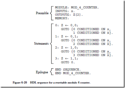
Figure 6-20 shows an HDL description of a modulo 4 counter. The counter produces the output sequence: 00, 01, 10, 11 and then repeats as long as the input line x is 0. If the input line is set to 1, then the counter returns to state 0 at the end of the next clock cycle. The comma is the catenation operator, and so the statement “Z ¬ 0,0;” assigns the two-bit pattern 00 to the two-bit output Z.
The HDL sequence is composed of three sections: the preamble, the numbered statements, and the epilogue. The preamble names the module with the “MODULE” keyword and declares the inputs with the “INPUTS” keyword, the outputs with the “OUTPUTS” keyword, and the arity (number of signals) of both, as well as any additional storage with the “MEMORY” keyword (none for this example). The numbered statements follow the preamble. The epilogue closes the sequence with the key phrase “END SEQUENCE.” The key phrase “END
MOD_4_COUNTER” closes the description of the module. Anything that appears between “END SEQUENCE” and “END MOD_4_COUNTER” occurs continuously, independent of the statement number. There are no such statements for this case.
In translating an HDL description into a design, the process can be decomposed into separate parts for the control section and the data section. The control section deals with how transitions are made from one statement to another. The data section deals with producing outputs and changing the values of any memory elements.
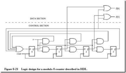
We consider the control section first. There are four numbered statements, and so we will use four flip-flops, one for each statement, as illustrated in Figure 6-21. This is referred to as a one-hot encoding approach, because exactly one flip-flop holds a true value at any time. Although four states can be encoded using only two flip-flops, studies have shown that the one-hot encoding approach results in approximately the same circuit area when compared with a more densely encoded approach; but more importantly, the complexity of the transfers from one state to the next are generally simpler and can be implemented with shallow combinational logic circuits, which means that the clock rate can be faster for a one-hot encoding approach than for a densely encoded approach.
In designing the control section, we first draw the flip-flops, apply labels as
appropriate, and connect the clock inputs. The next step is to simply scan the numbered statements in order and add logic as appropriate for the transitions. From statement 0, there are two possible transitions to statements 0 or 1, conditioned on x or its complement, respectively. The output of flip-flop 0 is thus connected to the inputs of flip-flops 0 and 1, through AND gates that take the value of the x input into account. Note that the AND gate into flip-flop 1 has a circle at one of its inputs, which is a simplified notation that means x is complemented by an inverter before entering the AND gate.
A similar arrangement of logic gates is applied for statements 1 and 2, and no logic is needed at the output of flip-flop 3 because statement 3 returns to statement 1 unconditionally. The control section is now complete and can execute correctly on its own. No outputs are produced, however, until the data section is implemented.
We now consider the design of the data section, which is trivial for this case. Both bits of the output Z change in every statement, and so there is no need to condition the generation of an output on the state. We only need to produce the correct output values for each of the statements. The least significant bit of Z is true in statements 1 and 3, and so the outputs of the corresponding control flip-flops are ORed to produce Z[0]. the most significant bit of Z is true in statements 2 and 3, and so the outputs of the corresponding control flip-flops are ORed to produce Z[1]. The entire circuit for the mod 4 counter is now complete, as shown in Figure 6-21.
We can now use our HDL in describing the control section of the ARC microarchitecture. There is no need to design the data section, since we have already defined its form in Figure 6-10. The data section is the same for both the micro- coded and hardwired approaches. As for the microcoded approach, the opera- tions that take place for a hardwired approach are:
1) Fetch the next instruction to be executed from memory.
2) Decode the opcode.
3) Read operand(s) from main memory or registers, if any.
4) Execute the instruction and store results.
5) Go to Step 1.
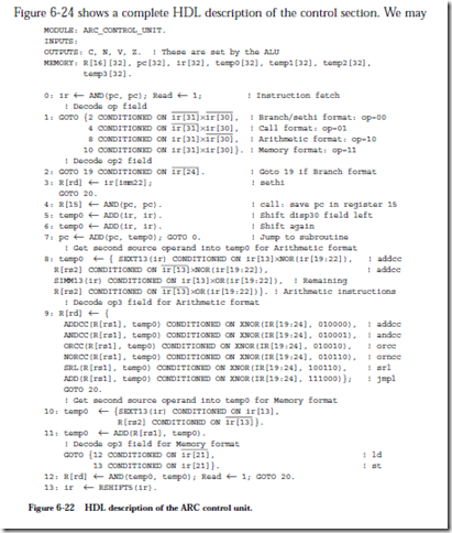
The microcode of Figure 6-15 can serve as a guide for what needs to be done. The first step is to fetch the next user-level instruction from main memory. The following HDL line describes this operation:
The structure of this statement is very similar to the first line of the microprogram, which may not be surprising since the same operations must be carried out on the same datapath.
Now that the instruction has been fetched, the next operation is to decode the opcode. This is where the power of a hardwired approach comes into play. Since every instruction has an op field, we can decode that field first, and then decode the op2, op3, and cond fields as appropriate for the instruction.
The next line of the control sequence decodes the op field:
The product symbol “X” indicates a logical AND operation. Control is thus transferred to one of the four numbered statements: 2, 4, 8, or 10 depending on the bit pattern in the op field.
have to do additional decoding depending on the value of the op field. At line 4, which is for the Call format, no additional decoding is necessary. The call instruction is then implemented in statements 4-7, which are similar to the microcoded version.
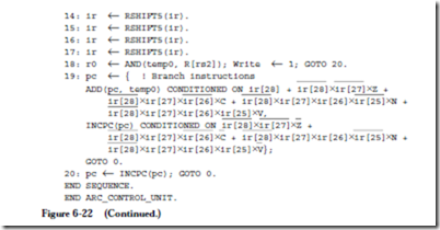
In statement 2, additional decoding is performed on the op2 field which is checked to determine if the instruction is sethi or a branch. Since there are only two possibilities, only one bit of op2 needs to be checked in line 2. Line 3 then implements sethi and line 19 implements the branch instructions.
Line 8 begins the Arithmetic format section of the code. Line 8 gets the second source operand, which can be either immediate or direct, and can be sign extended to 32 bits (for addcc) or not sign extended. Line 9 implements the Arithmetic format instructions, conditioned on the op3 field. The XNOR function returns true if its arguments are equal, otherwise it returns false, which is useful in making comparisons.
Line 10 begins the Memory format section of the code. Line 10 gets the second source operand, which can either be a register or an immediate operand. Line 11 decodes the op3 field. Since the only Memory format instructions are ld and st, only a single bit (IR[21]) needs to be observed in the op3 field. Line 12 then implements the ld instruction, and lines 13-18 implement the st instruction. Finally, line 20 increments the program counter and transfers control back to the first statement.
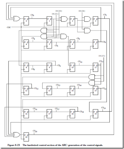
Now that the control sequence is defined, the next step is to design the logic for the control section. Since there are 21 statements, there are 21 flip-flops in the control section as shown in Figure 6-23. A control signal (CSi) is produced for each of the 21 states, which is used in the data section of the hardwired controller.
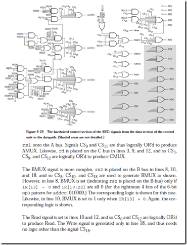
In Figure 6-24, the data section of the hardwired controller generates the signals that control the datapath. There are 27 OR gates that correspond to the 27 signals that control the datapath. (Refer to Figure 6-10. Count the 27 signals that originate in the control section that terminate in the datapath.) The AMUX signal is set to 1 only in lines 9 and 11, which correspond to operations that place
There are 4 signals that control the ALU: ALU[0], ALU[1], ALU[2], and ALU[3], which correspond to F0, F1, F2, and F3, respectively, in the ALU operation table shown in Figure 9-4. These four signals need values in each of the 20 HDL lines. In line 0, the ALU operation is AND, which corresponds to ALU[3:0] = 0101. Line 1 has no ALU operation specified, and so we can arbitrarily choose an ALU operation that has no side effects, like AND (0101). Continuing in this way, taking CONDITIONED ON statements into account, produces the logic for ALU[3:0] as shown in the figure.
The control signals are sent to the datapath, similar to the way that the MIR controls the datapath in the microprogrammed approach of Figure 6-10. The hard- wired and microcontrolled approaches can thus be considered interchangeable, except with varying costs. There are only 21 flip-flops in the hardwired approach, but there are 2048´41 = 83,968 flip-flops in the microprogrammed approach (although in actuality, a ROM would be used, which consumes less space because smaller storage elements than flip/flops can be used.) The amount of additional combinational logic is comparable. The hardwired approach is faster in executing ARC instructions, especially in decoding the Branch format instructions, but is more difficult to change once it is committed to fabrication.
EXAMPLE
Consider adding the same subcc instruction from the previous EXAMPLE to the hardwired implementation of the ARC instruction set. As before, the subcc instruction uses the Arithmetic format and an op3 field of 001100.
Only line 9 of the HDL code needs to be changed, by inserting the expression: ADDCC (R[rs1], INC_1(temp0)) CONDITIONED ON XNOR(IR[19:24], 001100), ! subcc before the line for addcc. The corresponding signals that need to be modified are ALU[3:0]. The INC_1 construct in the line above indicates that an adder CLU, which would be defined in another HDL module, should be created (in a hardwired control unit, there is a lot of flexibility on what can be done.)
