6.1 A Micro architecture for the ARC
In this section we consider a micro programmed approach for designing the ARC control unit. We begin by describing the data path and its associated control signals.
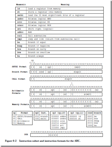
The instruction set and instruction format for the ARC subset is repeated from Chapter 4 in Figure 6-2. There are 15 instructions that are grouped into four for- mats according to the leftmost two bits of the coded instruction. The Processor Status Register % psr is also shown.
6.2.1 THE DATAPATH
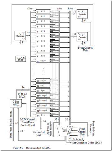
A datapath for the ARC is illustrated in Figure 6-3. The data path contains 32 user-visible data registers (%r0 – %r31), the program counter (%pc), the instruction register (%ir), the ALU, four temporary registers not visible at the ISA level (%temp0 – %temp3), and the connections among these components. The number adjacent to a diagonal slash on some of the lines is a simplification that indicates the number of separate wires that are represented by the corresponding single line.
Registers %r0 – %r31 are directly accessible by a user. Register %r0 always contains the value 0, and cannot be changed. The %pc register is the program counter, which keeps track of the next instruction to be read from the main memory. The user has direct access to %pc only through the call and jmpl instructions. The temporary registers are used in interpreting the ARC instruction set, and are not visible to the user. The %ir register holds the current instruction that is being executed. It is not visible to the user.
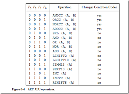
The ALU performs one of 16 operations on the A and B busses according to the table shown in Figure 6-4. For every ALU operation, the 32-bit result is placed on the C bus, unless it is blocked by the C bus MUX when a word of memory is placed onto the C bus instead.
The ANDCC and AND operations perform a bit-by-bit logical AND of corresponding bits on the A and B busses. Note that only operations that end with
“CC” affect the condition codes, and so ANDCC affects the condition codes whereas AND does not. (There are times when we wish to execute arithmetic and logic instructions without disturbing the condition codes.) The ORCC and OR operations perform a bit-by-bit logical OR of corresponding bits on the A and B busses. The NORCC and NOR operations perform a bit-by-bit logical NOR of corresponding bits on the A and B busses. The ADDCC and ADD operations carry out addition using two’s complement arithmetic on the A and B busses.
The SRL (shift right logical) operation shifts the contents of the A bus to the right by the amount specified on the B bus (from 0 to 31 bits). Zeros are copied into the leftmost bits of the shifted result, and the rightmost bits of the result are discarded. LSHIFT2 and LSHIFT10 shift the contents of the A bus to the left by two and 10 bits, respectively. Zeros are copied into the rightmost bits.
SIMM13 retrieves the least significant 13 bits of the A bus, and places zeros in the 19 most significant bits. SEXT13 performs a sign extension of the 13 least significant bits on the A bus to form a 32-bit word. That is, if the leftmost bit of the 13 bit group is 1, then 1’s are copied into the 19 most significant bits of the result, otherwise, 0’s are copied into the 19 most significant bits of the result. The INC operation increments the value on the A bus by 1, and the INCPC operation increments the value on the A bus by four, which is used in incrementing the PC register by one word (four bytes). INCPC can be used on any register placed on the A bus.
The RSHIFT5 operation shifts the operand on the A bus to the right by 5 bits, copying the leftmost bit (the sign bit) into the 5 new bits on the left. This has the effect of performing a 5-bit sign extension. When applied three times in succession to a 32-bit instruction, this operation also has the effect of placing the left- most bit of the COND field in the Branch format (refer to Figure 6-2) into the position of bit 13. This operation is useful in decoding the Branch instructions, as we will see later in the chapter. The sign extension for this case is inconsequential.
Every arithmetic and logic operation can be implemented with just these ALU operations. As an example, a subtraction operation can be implemented by forming the two’s complement negative of the subtrahend (making use of the NOR operation and adding 1 to it with INC) and then performing addition on the operands. A shift to the left by one bit can be performed by adding a number to itself. A “do-nothing” operation, which is frequently needed for simply passing data through the ALU without changing it, can be implemented by logically ANDing an operand with itself and discarding the result in %r0. A logical XOR can be implemented with the AND, OR, and NOR operations, making use of DeMorgan’s theorem (see problem 6.5).
The ALU generates the c, n, z, and v condition codes which are true for a carry, negative, zero, or overflow result, respectively. The condition codes are changed only for the operations indicated in Figure 6-4. A signal (SCC) is also generated that tells the %psr register when to update the condition codes.
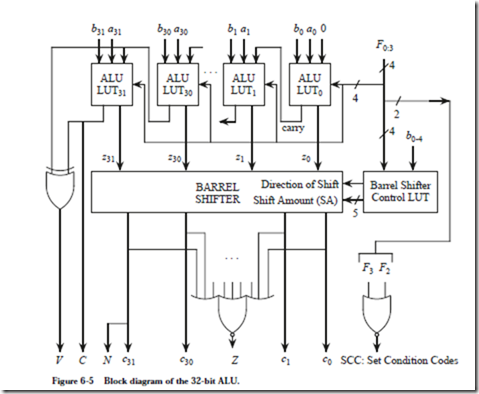
The ALU can be implemented in a number of ways. For the sake of simplicity, let us consider using a lookup table (LUT) approach. The ALU has two 32-bit data inputs A and B, a 32-bit data output C, a four-bit control input F, a four-bit condition code output (N, V, C, Z), and a signal (SCC) that sets the flags in the
%psr register. We can decompose the ALU into a cascade of 32 LUTs that implement the arithmetic and logic functions, followed by a barrel shifter that implements the shifts. A block diagram is shown in Figure 6-5.
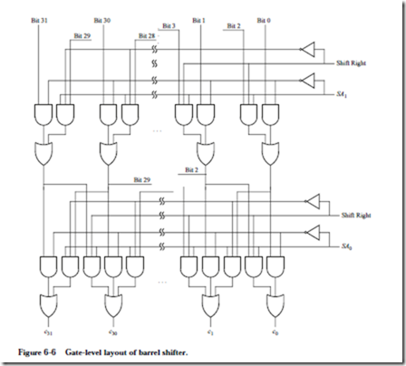
The barrel shifter shifts the input word by an arbitrary amount (from 0 to 31 bits) according to the settings of the control inputs. The barrel shifter performs shifts in levels, in which a different bit of the Shift Amount (SA) input is observed at each level. A partial gate-level layout for the barrel shifter is shown in
Figure 6-6. Starting at the bottom of the circuit, we can see that the outputs of the bottom stage will be the same as the inputs to that stage if the SA0 bit is 0. If the SA0 bit is 1, then each output position will take on the value of its immediate left or right neighbor, according to the direction of the shift, which is indicated by the Shift Right input. At the next higher level, the method is applied again, except that the SA1 bit is observed and the amount of the shift is doubled. The process continues until bit SA4 is observed at the highest level. Zeros are copied into positions that have no corresponding inputs. With this structure, an arbitrary shift from 0 to 31 bits to the left or the right can be implemented.
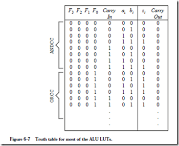
Each of the 32 ALU LUTs is implemented (almost) identically, using the same lookup table entries, except for changes in certain positions such as for the INC and INCPC operations (see problem Figure 6.20). The first few entries for each LUT are shown in Figure 6-7. The barrel shifter control LUT is constructed in a similar manner, but with different LUT entries.
The condition code bits n, z, v, and c are implemented directly. The n and c bits are taken directly from the c31 output of the barrel shifter and the carry-out position of ALU LUT31, respectively. The z bit is computed as the NOR over the barrel shifter outputs. The z bit is 1 only if all of the barrel shifter outputs are
0. The v (overflow) bit is set if the carry into the most significant position is different than the carry out of the most significant position, which is implemented with an XOR gate.
Only the operations that end in “CC” should set the condition codes, and so a signal is generated that informs the condition codes to change, as indicated by the label “SCC: Set Condition Codes.” This signal is true when both F3 and F2 are false.
The Registers
All of the registers are composed of falling edge-triggered D flip-flops (see Appen-
dix A). This means that the outputs of the flip-flops do not change until the clock makes a transition from high to low (the falling edge of the clock). The registers all take a similar form, and so we will only look at the design of register
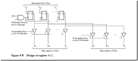
%r1. All of the datapath registers are 32 bits wide, and so 32 flip-flops are used for the design of %r1, which is illustrated in Figure 6-8.
The CLK input to register %r1 is ANDed with the select line (c1) from the C Decoder. This ensures that %r1 only changes when the control section instructs it to change. The data inputs to %r1 are taken directly from the corresponding
lines of the C bus. The outputs are written to the corresponding lines of the A and B busses through tri-state buffers, which are “electrically disconnected” unless their enable inputs are set to 1. The outputs of the buffers are enabled onto the A and B busses by the a1 and b1 outputs of the A and B decoders, respectively. If neither a1 nor b1 are high (meaning they are equal to 1), then the outputs of %r1 are electrically disconnected from both the A and B busses since the tri-state buffers are disabled.
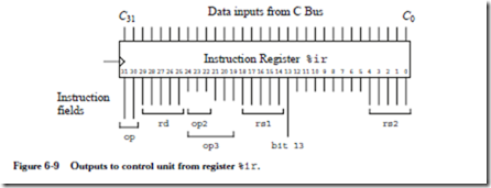
The remaining registers take a similar form, with a few exceptions. Register %r0 always contains a 0, which cannot be changed. Register %r0 thus has no inputs from the C bus nor any inputs from the C decoder, and does not need flip-flops (see Problem 6.11). The %ir register has additional outputs that correspond to the rd, rs1, rs2, op, op2, op3, and bit 13 fields of an instruction, as illustrated in Figure 6-9. These outputs are used by the control section in interpreting
an instruction as we will see in Section 6.2.4. The program counter can only contain values that are evenly divisible by 4, and so the rightmost two bits in %pc can be hardwired to 0.
The A, B, and C decoders shown in Figure 6-3 simplify register selection. The six-bit inputs to the decoders select a single register for each of the A, B, and C busses. There are 26 = 64 possible outputs from the decoders, but there are only 38 data registers. The index shown to the left of each register (in base 10) in Figure 6-3 indicates the value that must be applied to a decoder input to select the corresponding register. The 0 output of the C decoder is not used because %r0 cannot be written. Indices that are greater than 37 do not correspond to any registers, and are free to be used when no registers are to be connected to a bus.
6.2.2 THE CONTROL SECTION
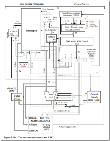
The entire microprogrammed ARC microarchitecture is shown in Figure 6-10.
The figure shows the datapath, the control unit, and the connections between them. At the heart of the control unit is a 2048 word ´ 41 bit read-only memory (ROM) that contains values for all of the lines that must be controlled to implement each user-level instruction. The ROM is referred to as a control store in this context. Each 41-bit word is called a microinstruction. The control unit is responsible for fetching microinstructions and executing them, much in the same way as user-level ARC macroinstructions are fetched and executed. This microinstruction execution is controlled by the microprogram instruction register (MIR), the processor status register (%psr), and a mechanism for determining the next microinstruction to be executed: the Control Branch Logic (CBL) unit and the Control Store (CS) Address MUX. A separate PC for the microprogram is not needed to store the address of the next microinstruction, because it is recomputed on every clock cycle and therefore does not need to be stored for future cycles.
When the microarchitecture begins operation (at power-on time, for example), a reset circuit (not shown) places the microword at location 0 in the control store into the MIR and executes it. From that point onward, a microword is selected for execution from either the Next, the Decode, or the Jump inputs to the CS Address MUX, according to the settings in the COND field of the MIR and the output of the CBL logic. After each microword is placed in the MIR, the datapath performs operations according to the settings in the individual fields of the MIR. This process is detailed below.
A microword contains 41 bits that comprise 11 fields as shown in Figure 6-11.
Starting from the left, the A field determines which of the registers in the datapath are to be placed on the A bus. The bit patterns for the registers correspond to the binary representations of the base 10 register indices shown in Figure 6-3 (000000 – 100101). The AMUX field selects whether the A Decoder takes its input from the A field of the MIR (AMUX = 0) or from the rs1 field of %ir (AMUX = 1).
In a similar manner, the B field determines which of the registers in the datapath are to be placed on the B bus. The BMUX field selects whether the B Decoder takes its input from the B field of the MIR (BMUX = 0) or from the rs2 field of %ir (BMUX = 1). The C field determines which of the registers in the datapath is to be written from the C bus. The CMUX field selects whether the C Decoder takes its input from the C field of the MIR (CMUX = 0) or from the rd field of %ir (CMUX = 1). Since %r0 cannot be changed, the bit pattern 000000 can be used in the C field when none of these registers are to be changed.
The RD and WR lines determine whether the memory will be read or written, respectively. A read takes place if RD = 1, and a write takes place if WR = 1. Both the RD and WR fields cannot be set to 1 at the same time, but both fields can be 0 if neither a read nor a write operation is to take place. For both RD and WR, the address for the memory is taken directly from the A bus. The data input to the memory is taken from the B bus, and the data output from the memory is placed on the C bus. The RD line controls the 64-to-32 C Bus MUX, which determines whether the C bus is loaded from the memory (RD = 1) or from the ALU (RD = 0).
The ALU field determines which of the ALU operations is performed according to the settings shown in Figure 6-4. All 16 possible ALU field bit patterns correspond to valid ALU operations. This means that there is no way to “turn the ALU off ” when it is not needed, such as during a read or write to memory. For this situation, an ALU operation should be selected that has no unwanted side effects. For example, ANDCC changes the condition codes and would not be appropriate, whereas the AND operation does not affect the condition codes, and would therefore be appropriate.
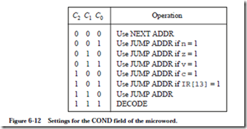
The COND (conditional jump) field instructs the microcontroller to take the next microword from either the next control store location, or from the location in the JUMP ADDR field of the MIR, or from the opcode bits of the instruction in %ir. The COND field is interpreted according to the table shown in Figure 6-12. If the COND field is 000, then no jump is taken, and the Next input to the CS Address MUX is used. The Next input to the CS Address MUX is computed by the control store address incrementer (CSAI) shown in Figure 6-10, which increments the current output of the CS Address MUX by 1. If the COND field is 001, 010, 011, 100, or 101, then a conditional jump is taken to the control store location in the JUMP ADDR field, according to the value of the n, z, v, or c flags, or bit 13 of %ir, respectively. The syntax “IR[13]” means “bit 13 of the instruction register %ir.” If the COND field is 110, then an unconditional jump is taken.
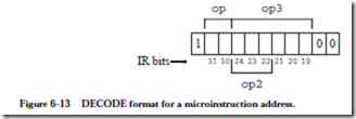
The bit pattern 111 is used in the COND field when an instruction is being decoded. When the COND field is 111, then the next control store location that is copied into the MIR is taken from neither the Next input to the CS Address MUX nor the Jump input, but is taken from a combination of 11 bits created by appending 1 to the left of bits 30 and 31 of %ir and appending 00 to the right of bits 19-24 of %ir. This DECODE address format is shown in Figure 6-13. The
purpose of using this addressing scheme is to allow an instruction to be decoded in a single step, by branching to a different location according to the settings in the op, op2, and op3 fields of an instruction.
Finally, the JUMP ADDR field appears in the rightmost 11 bits of the micro- word format. There are 211 microwords in the control store, and so 11 bits are needed in the JUMP ADDR field in order to jump to any microstore location.
