MC68020 System Design
The following 8-MHz 68020 system design will use a 128 KB 32-bit wide supervisor data memory. Four 27C256’s (32K x 8 HCMOS EPROM with 120-ns access time) are used for this purpose. Because the memory is 32 KB, the 68020 address lines A2-A16 are used for addressing the 27C256′ s. The 68020 SIZ1, SIZ0, A 1, A0, DSACK 1, and DSACK0 pins are utilized for selecting the memory chips.
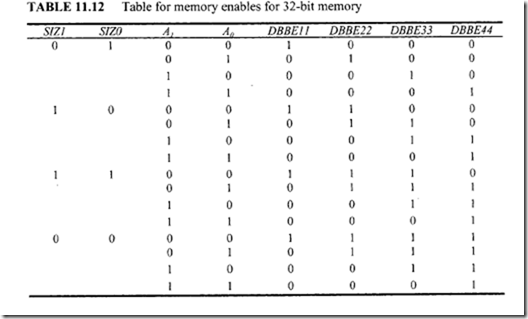
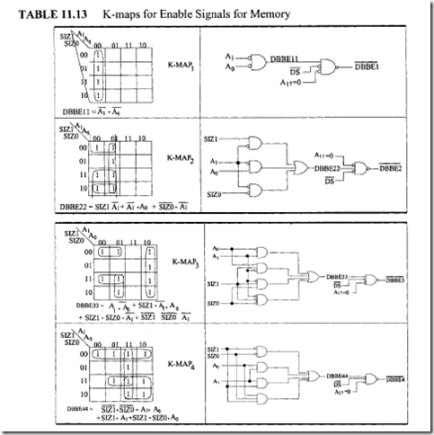
Table 11.12 shows the table for designing the enable logic for the four 27C256 chips. The 68020 A 17 pin is used to distinguish between memory and I/O. A 17 = 0 is used to select the memory chips; A 17 = 1 is used to select I/O chips (not shown in the design). Table 11.13 shows the K-maps for the enable logic. A logic diagram can be drawn for generating the memory byte enable signals DBBE1, DBBE2, DBBE3, and DBBE4.
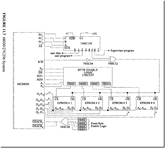
The 68020 system with 32-bit memory consists offour 27C256’s, each connected to its associated portion of the system data bus (D31-D24 , D23-D16, D15-D8, and D7-D0).
To manipulate this memory configuration, 32-bit data bus control byte enable logic is incorporated to generate byte enable signals (DBBE1, DBBE2, DBBE3, and DBBE4). These byte enables are generated by using 68020’s SIZ1, SIZ0, A 1, A0, A 17, and DS pins as shown in the individual logic diagrams of the byte enable logic. A PAL can be programmed to implement this logic. A schematic of the 68020-27C256 interface is shown in Figure 11.7.
Because the 68020 clock is used to generate DSACK1, and DSACKO, the 68020 operates in synchronous mode.
A 74HC138 decoder is used for selecting memory banks to enable the appropriate memory chips. The 74HCI38 is enabled by AS= 0. The output line 5 (FC2FC1FC0 = 101 for supervisor data) is used to select the memory chips. Assuming don’t cares to be zeros and also note that A 17 = 0 for memory, the supervisor data memory map is obtained as follows:
and DBBE4 outputs of the byte enable logic circuit. When one or more EPROM chips are selected, the appropriate enables (DBBE1-DBBE4) will be low, thus asserting DSACK1 = 0 and DSACKO = 0. This will tell the 68020 that the memory is 32 bits wide. Data from the selected memory chip(s) will be placed on the appropriate data pins of the 68020. For example, in response to execution of the instruction MOVE • W $ 0 0 0 0 0 0 0 1,D0 in the supervisor mode, the 68020 will generate appropriate signals to generate DBBEl- 1, DBBE2= 0, DBBE3= 0, DBBE4= 1, RIW = 1, and output 5 of the decoder= 0 This will select EPROM #2 and EPROM #3 chips. Thus, the contents of address $00000001 are transferred to DO (bits 8-15) and the contents of address $00000002 are moved to DO (bits 0-7). The supervisor program, user program, and user data memories can be connected in a similar way (not shown in the figure). For each memory space, four memory chips are required.
Let us discuss the timing requirements of the 68020/27C256 system. Because the 68020 clock is used to generate DSACKl and DSACKO, the 68020 operates in synchronous mode. This means that the 68020 checks DSACK 1 and DSACKO for LOW at the falling edge of S2 (two cycles). From the 68020 timing diagram (Motorola manual), AS, DS, and all other output signals used in memory decoding go to LOW at the end of approximately one clock cycle. For an 8-MHz 68020 clock, each cycle is 125 ns. From byte enable logic diagrams, a maximum of four gate delays (40 ns) are required. Therefore, the selected EPROM(s) will be enabled after 165 ns (125 ns + 40 ns). With 120-ns access time, the EPROM(s) will place data on the output lines after approximately 285 ns (165 ns + 120 ns). With an 8-MHz 68020 clock, DSACKl and DSACKO will be checked for LOW (32-bit memory) after two cycles (250 ns) and if LOW, the 68020 wi111atch data after three cycles (375 ns). Hence, no delay circuit is required for DSACK1 and DSACKO..In case a delay circuit is required, a ring counter can be used. Note that the 20-ns window requirement for DSACK1 and DSACKO inputs (5 ns before and 15 ns after the falling edge of S2) is satisfied.
MC68020 I/O
The 68020 I/O handling features are very similar to those of the 68000. This means that the 68020 uses memory-mapped I/O, and the 68230 I/O chip can be used for programmed I/O. The external interrupts are handled via the 68020 IPL2, IPLI, and IPLO pins using autovectoring and nonautovectoring pins. However, the 68020 uses a new pin called AVEC rather than VPA (68HC000) for autovectoring. Nonautovectoring is handled using DSACKO = 0 and DSACK1 = 0 rather than DTACKO= 0 (as with the 68HC000). Note that the 68020 does not have the VPA pin. Like the 68HC000, the 68020 uses the BR, BG, and BGACK pins for DMA transfer. The 68020 exceptions are similar to those of the 68000 with some variations such as coprocessor exceptions.


