11.6 Merced/IA-64
Intel and Hewlett-Packard recently announced a 64-bit microprocessor called "Merced" and also known as "Intel Architecture-64" (IA-64) or ltanium. The microprocessor is not an extension of Intel’s 32-bit 80×86 or Pentium series processors, nor is it an evolution of HP’s 64-bit RISC architecture. IA-64 is a new design that will implement innovative forward-looking features to help improve parallel instruction processing: that is, long instruction words, instruction prediction, branch elimination, and speculative loading. These techniques are not necessarily new concepts, but they are implemented in ways that are much more efficient.
An 80×86 instruction varies in length from 8 to 108 bits, and the microprocessor spends time and work decoding each instruction while scanning for the instruction boundaries during execution. In addition, Pentium processors frantically try to reorder instructions and group them so that two instructions can be fed into two processing pipelines simultaneously. Although improving performance, this approach is still rather ineffective and has a high cost of logic circuitry in the chip.
The IA-64 packs three instructions into a single 128-bit bundle-something Intel calls "explicitly parallel instruction computing" (EPIC). During compilation of a program, the compiler explicitly tells the microprocessor inside the 128-bit packet which of the instructions can be executed in parallel. Hence, the microprocessor does not need to scramble at run-time to discover and reorder instructions for parallel execution because all of this has already been done at compilation. While trying to keep the instruction pipeline full, 80×86 or Pentium family processors try to predict which way branches will take place and speculatively execute instructions along the predicted path. In case of wrong guesses, the microprocessor must discard the speculative results, flush the pipelines, and reload the correct instructions into the pipe. This results in a large loss of microprocessor cycles.
In dealing with branch prediction, the IA-64 puts the burden on the compiler. Wherever practical, the compiler inserts flags into the instruction packets to mark separate paths from a branch instruction. These flags, known as "predicates," allow the microprocessor to funnel instructions for a specific branch into a pipe and execute each branch separately and simultaneously. This effectively lets the microprocessor process different paths of a branch at the same time, then discard the results of the path it does not need.
One drawback of the 80×86 processor series is the fact that data is not fetched from memory until the microprocessor needs it and calls for it. The IA-64 implements speculative loading, which allows the memory and I/O devices to be delivering data to the microprocessor before the processor actually needs it, eliminating some of the delays the 80×86 processor incurs while waiting for data to appear on the bus.
During compilation of a program, the compiler scans the source code and when it sees an upcoming load instruction, removes it and inserts a speculative load instruction a few cycles ahead of it. In this manner, the IA-64 is able to continue executing code while minimizing delay time that the memory or I/O devices inherently incur.
11.7 Overview of Motorola 32- and 64-bit Microprocessors
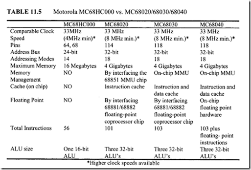
This section provides an overview of the state-of-the-art in Motorola’s microprocessors. Motorola’s 32-bit microprocessors based on 68HC000 architecture include the MC68020, MC68030, MC68040, and MC68060. Table 11.5 compares the basic features of some of these microprocessors with the 68HC000.
The PowerPC family of microprocessors were jointly developed by Motorola, IBM, and Apple. The PowerPC family contains both 32- and 64-bit microprocessors. One of the noteworthy feature of the PowerPC is that it is the first top-of-the-line microprocessor to include an on-chip real-time clock (RTC). The RTC is common in single-chip microcomputers rather than microprocessors. The PowerPC is the first microprocessor to implement this on-chip feature, which makes it easier to satisfy the requirements of time keeping for task switching and calendar date of modem multitasking operating systems. The PowerPC microprocessor supports both the Power Mac and standard PCs. The PowerPC family is designed using RISC architecture
11.7.1 Motorola MC68020
The MC68020 is Motorola’s first 32-bit microprocessor. The design of the 68020 is based on the 68HC000. The 68020 can perform a normal read or write cycle in 3 clock cycles without wait states as compared to the 68HC000, which completes a read or write operation in 4 clock cycles without wait states. As far as the addressing modes are concerned, the 68020 includes new modes beyond those of the 68HC000. Some of these modes are scaled indexing, larger displacements, and memory indirection. Furthermore, several new instructions are added to the 68020 instruction set, including the following:
-
Bit field instructions are provided for manipulating a string of consecutive bits with a variable length from 1 to 32 bits.
-
Two new instructions are used to perform conversions between packed BCD and ASCII or EBCDIC digits. Note that a packed BCD is a byte containing two BCD digits.
-
Enhanced 68000 array-range checking (CHK2) and compare (CMP2) instructions are included. CHK2 includes lower and upper bound checking; CMP2 compares a number with lower and upper values and affects flags accordingly.
-
Two advanced instructions, namely, CALLM and RTM, are included to support modular programming.
-
Two compare and swap instructions (CAS and CAS2) are provided to support multiprocessor systems.
A comparison of the differences between the 68020 and 68HCOOO will be provided later in this section.
The 68030 and 68040 are two enhanced versions of the 68020. The 68030 retains most of the 68020 features. It is a virtual memory microprocessor containing an on-chip MMU (memory management unit). The 68040 expands the 68030 on-chip memory management logic to two units: one for instruction fetch and one for data access. This speeds up the 68040’s execution time by performing logical-to-physical-address translation in parallel. The on-chip floating-point capability of the 68040 provides it with both integer and floating-point arithmetic operations at a high speed. All 68HC000 programs written in assembly language in user mode will run on the 68020/68030 or 68040. The 68030 and 68040 support all 68020 instructions except CALLM and RTM. Let us now focus on the 68020 microprocessor in more detail.
MC68020 Functional Characteristics
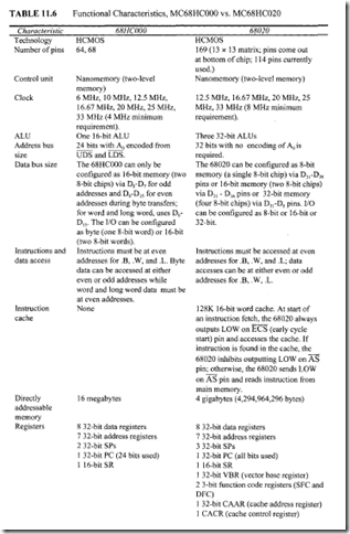
The MC68020 is designed to execute all user object code written for the 68HC000. Like the 68HCOOO, it is manufactured using HCMOS technology. The 68020 consumes a maximum of 1.75 W. It contains 200,000 transistors on a 3/8" piece of silicon. The chip is packaged in a square ( 1.345" x 1.345") pin grid array (PGA) and other packages. It contains 169 pins (114 pins used) arranged in a 13 x 13 matrix.
The processor speed of the 68020 can be 12.5, 16.67, 20, 25, or 33 MHz. The chip must be operated from a minimum frequency of 8 MHz. Like the 68HC000, it does not have any on-chip clock generation circuitry. The 68020 contains 18 addressing modes and 101 instructions. All addressing modes and instructions ofthe 68HC000 are included in the 68020. The 68020 supports coprocessors such as the MC68881/MC68882 floating-point and MC68851 MMU coprocessors.
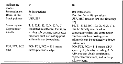
These and other functional characteristics of the 68020 are compared with the 68HC000 in Table 11.6. Some of the 68020 characteristics in Table 11.6 will now be explained.
-
Three independent ALUs are provided for data manipulation and address calculations
-
A 32-bit barrel shift register (occupies 7% of silicon) is included in the 68020 for very fast shift operations regardless of the shift count.
-
The 68020 has three SPs. In the supervisor mode (when S = 1), two SPs can be accessed. These are MSP (when M = 1) and ISP (when M = 0). ISP can be used to simplify and speed up task switching for operating systems.
-
The vector base register (VBR) is used in interrupt vector computation. For example, in the 68HC000, the interrupt vector address is obtained by using VBR + 4 x 8-bit vector.
-
The SFC (source function code) and DFC (destination function code) registers are 3 bits wide. These registers allow the supervisor to move data between address spaces. In supervisor mode, 3-bit addresses can be written into SFC or DFC using such instructions such as MOVEC A2, SFC. The upper 29 bits of SFC are assumed to be zero. The MOVES. W (AO) , DO can then be used to move a word from a location within the address space specified by SFC and [AO] to DO. The 68020 outputs [SFC] to the FC2, FC I, and FCO pins. By decoding these pins via an external decoder, the desired source memory location addressed by [AO] can be accessed.
-
The new addressing modes in the 68020 include scaled indexing, 32-bit displacements, and memory indirection. To illustrate the concept of scaling, consider moving the contents of memory location 5010 to Al. Using the 68000, the following instruction sequence will accomplish this
-
The new 68020 instructions include bit field instructions to better support compilers and certain hardware applications such as graphics, 32-bit multiply and divide instructions, pack and unpack instructions for BCD, and coprocessor instructions. Bit field instructions can be used to input AID converters and eliminate wasting main memory space when the AID converter is not 32 bits wide. For example, if the AID is 12 bits wide, then the instruction BFEEXTU $22 32 0 0 0 0 { 2: 13}, DO will input bits 2-13 of memory location $22320000 into DO. Note that $22320000 is the memory-mapped port, where the 12-bit AID is connected at bits 2-13. The next AID can be connected at bits 14-25, and so on.
-
FC2, FC 1, FCO = 111 means CPU space cycle. The 68020 makes CPU space access for breakpoints, coprocessor operations, or interrupt acknowledge cycles. The CPU space classification is generated by the 68020 based upon execution of breakpoint instructions or coprocessor instructions, or during an interrupt acknowledge cycle. The 68020 then decodes A 16-A19 to determine the type of CPU space. For example, FC2, FC1, FCO = 111 and A 19, A, 8 , A 17, A,6 = 0010 mean coprocessor instruction.
-
For performing floating-point operation, the 68HC000 user must write subroutines using the 68HC000 instruction set. The floating-point capability in the 68020 can be obtained by connecting a floating-point coprocessor chip such as the Motorola 68881. The 68020 has two coprocessor chips: the 68881 (floating point) and the 68851 (memory management). The 68020 can have up to eight coprocessor chips. When a coprocessor is connected to the 68020, the coprocessor instructions are added to the 68020 instruction set automatically, and this is transparent to the user. For example, when the 68881 floating-point coprocessor is added to the 68020, instructions such as FADD (floating-point add) are available to the user. The programmer can then execute the instruction FADD FDO, FDl. Note that registers FDO and FD1 are in the 68881. When the 68020 encounters the FADD instruction, it writes a command in the command register in the 68881, indicating that the 68881 has to perform this operation. The 68881 then responds to this by writing in the 68881 response register. Note that all coprocessor registers are memory mapped. Hence, the 68020 can read the response register and obtain the result of the floating-point add from the appropriate locations.
-
The 68HC000 DTACK pin is replaced by two pins on the 68020: DSACK1 and DSACKO. These pins are defined as follows:
The 68020 can be configured as a byte, 16-bit, or 32-bit memory system. As a byte memory system, the data pins of a single 8-bit memory containing all addresses in increments of one can be connected to the 68020 D31-D24 pins. All data transfers occur via pins D31-D24. The byte memory chip informs the 68020 of its size by activating DSACK1 = 1 and DSACKO = 0 so that the 68020 transfers data via its D31-D24 pins.
For byte instructions, one byte is transferred via these pins; for word (16-bit) instructions, two consecutive bytes are transferred via these pins; for long word (32-bit) instructions, four consecutive bytes are transferred via these pins.
When the 68020 is configured as a word (16-bit) memory system, two byte memory chips are interfaced to the 68020 via its D31- D16 pins. The data pins of the byte memory chips containing even and odd addresses are connected to the 68020 pins D31- D24 and D23-D16, respectively. The memory chips inform the 68020 of the 16-bit memory configuration by activating DSACK1 = 0 and DSACKO = 1. The 68020 then uses D31-D16 to transfer data for byte, word, or long word instructions. For byte instructions, one byte is transferred via pins D31-D24 or D23-D16 depending on whether the address is even or odd. For word instructions, the contents of both even and odd addresses are transferred via pins D31-D16 with even-address byte via D31 -D24 pins and odd-addressed byte via D23 -D16 pins; for long word instructions, four consecutive bytes are transferred via pins D31-D16 with the contents of even addresses via pins D31-D16 using additional cycles. Data transfer can be aligned or misaligned. For 16-bit memory systems, a word or long word instruction with data transfer starting at an even address is called an "aligned transfer." For example, the instruction MOVE .w D1, $ 3 0 0 0 0 0 0 0 will store one data byte at the even address $30000000 via pins D31-D24 and one data byte at the odd address $30000001 via pins D23-D16 in one cycle. On the other hand, MOVE. W DO, $3 0 0 0 0 0 01 is a misaligned transfer. The 68020 transfers one byte to $30000001 via pins D23-D16 in the first cycle and another byte to $30000002 via pins D31-D24 in the second cycle. Thus, the misaligned transfer for word instruction takes two cycles in a 16-bit memory configuration. For 32- bit transfers, MOVE .L D1, $ 3 0 0 0 0 0 0 0 is an aligned transfer. During the first cycle, the 68020 transfers 8-bit contents of the highest byte of DO to $30000000 via pins D31- D24, and the next 8-bit contents of DO to $30000001 via pins D23-D16. During the second cycle, the 68020 transfers next byte of DO to $30000002 via pins D31-D24 and the lowest byte of register DO to $30000003 via pins D23-D16. Thus, for aligned transfer with 16-bit memory configuration, the 68020 transfers data in two cycles for 32-bit transfers. Next, consider the instruction, MOVE. L DO, $30000001. This is a misaligned transfer. The 68020 transfers the most significant byte of DO to $30000001 via pins D23-D16 in the first cycle, the next byte of register DO to $30000002 via pins D31-D24, and the next byte of D0 to $30000003 via pins D23-D16 in the second cycle and finally, the lowest byte of D0 to address $30000004 via pins D31-D24 in the third cycle. Thus, for misaligned transfers in a 16- bit memory configuration, the 68020 requires 3 cycles to transfer data for long word instructions.
When the 68020 is configured as a 32-bit memory system, four byte memory chips are connected to D31-D0 • The memory chip with data pins connected to D3 ,-D24 contains addresses 0, 4, 8, …; the,memory chip with data pins connected to D23-D16 contains addresses 1, 5, 9, …; the memory chip with data pins connected to D15-D8 includes addresses 2, 6, 10, …;and the memory chip with data pins connected to D7-D0 contains addresses 3, 7, 11, …. The memory chips inform the 68020 of the 32-bit memory configuration by activating DSACK1 = 0 and DSACKO = 0. The 68020 then uses pins D31-D0 to transfer data for byte, word, or long word instructions. For byte instructions, data is transferred via the appropriate 8 data pins of the 68020 depending on the address in one cycle. For word instructions starting at addresses 0, 4, 8, …,addresses 1, 5, 9, …,and addresses 2, 6, 10, …, data are aligned, and will be transferred in one cycle. For example, consider MOVE .W D1,$2 0 0 0 0 0 0 5. The 68020 transfers the contents of D 1 (bits 15-8) to address $20000005 via pins D23-D16 and contents of register Dl (bits 7-0) to address $20000006 via pins D 15-D8 in one cycle. On the other hand, MOVE • W D1,$2 0 0 0 0 0 0 7 is a misaligned transfer. In this case, the 68020 transfers the contents of register D 1 (bits 15-8) to address $20000007 via pins DrD0 in the first cycle and the contents of D1 (bits 7-0) to address $20000008 via pins D31-D24 in the second cycle.
For long word instructions, data transfers with addresses starting at 0, 4, 8, … are aligned transfers. They will be performed in one cycle. Data with addresses in all other three chips are misaligned and will require additional cycles. For I/O configuration, one to four chips can be connected to the appropriate D31-D0 pins as required by an application.
The addresses in the I/O chips will be memory mapped and connected to the appropriate portions of pins D31-D0 in the same way as the memory chips.
MC68020 Programmer’s Model
The MC68020 programmer’s model is based on sequential, nonconcurrent instruction execution. This implies that each instruction is completely executed before the next instruction is executed. Although instructions might operate concurrently in actual hardware, they do not operate concurrently in the programmer’s model.
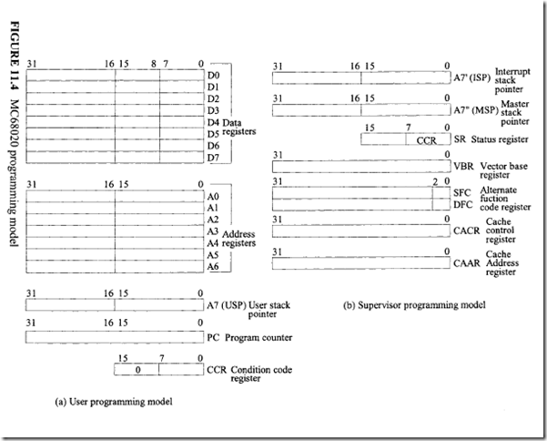
Figure 11.4 shows the MC68020 user and supervisor programming models. The user model has fifteen 32-bit general-purpose registers (D0-D7 and A0-A6), a 32-bit program counter (PC), and a condition code register (CCR) contained within the supervisor status register (SR). The supervisor model has two 32-bit supervisor stack pointers (ISP and MSP), a 16-bit status register (SR), a 32-bit vector base register (VBR), two 3-bit
alternate function code registers (SFC and DFC), and two 32-bit cache-handling (address and control) registers (CAAR and CACR). The user stack pointer (USP) A 7, interrupt stack pointer (ISP) A7′, and master stack pointer (MSP) A7” are system stack pointers.
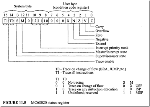
The status register, as shown in Figure 11.5, consists of a user byte (condition code register, CCR) and a system byte. The system byte contains control bits to indicate that the processor is in the trace mode (T1, T0), supervisor/user state (S), and master/interrupt state (M). The user byte consists of the following condition codes: carry (C), overflow (V), zero (Z), negative (N), and extend (X).
The bits in the 68020 user byte are set or reset in the same way as those of the 68HC000 user byte. Bits 12, Il, IO, and Shave the same meaning as those of the 68HC000. In the 68020, two trace bits (Tl, TO) are included as opposed to one trace bit (T) in the 68HCOOO. These two bits allow the 68020 to trace on both normal instruction execution and jumps. The 68020 M bit is not included in the 68HC000 status register.
The vector base register (VBR) is used to allocate the exception processing vector table in memory. VBR supports multiple vector tables so that each process can properly manage independent exceptions. The 68020 distinguishes address spaces as supervisor/ user and program/data. To support full access privileges in the supervisor mode, the alternate function code registers (SFC and DFC) allow the supervisor to access any address space by preloading the SFC/DFC registers appropriately. The cache registers (CACR and CAAR) allow software manipulation of the instruction code. The CACR provides control and status accesses to the instruction cache; the CAAR holds the address for those cache control functions that require an address.
