9.9.3 8086 I/O Ports
Devices with 8-bit I/O ports can be connected to either the upper or the lower half of the data bus. If the I/O port chip is connected to the lower half of the 8086 data lines (AD0- AD7), the port addresses will be even (A0 = 0). On the other hand, the port addresses will be odd (A0 = 1) if the I/O port chip is connected to the upper half of the 8086 data lines (AD8-AD 15). A0 will always be 1 or 0 for the partitioned I/O chip. Therefore, A0 cannot be used as an address input to select registers within a particular I/O chip. If two chips are connected to the lower and upper halves of the 8086 address bus that differ only in A0 (consecutive odd and even addresses), A0 and BHE must be used as conditions of chip select decoding to avoid a write to one I/O chip from erroneously performing a write to the other.
The 8086 uses either standard I/O or memory-mapped I/O. The standard I/O uses the instructions IN and OUT, and is able to provide up to 64K bytes of I/O locations. The standard I/O can transfer either 8-bit data or 16-bit data to or from a peripheral device. The 64-Kbyte I/O locations can then be configured as 64K 8-bit ports or 32K 16-bit ports. All I/O transfers between the 8086 and peripheral devices take place via AL for 8-bit ports (AH is not involved) and AX for 16-bit ports.
The I/O port addressing can be done either directly or indirectly as follows:
• Direct
IN AX, PORTA or IN AL, PORTA inputs 16-bit contents of port A into AX or 8-bit contents of port A into AL, respectively.
OUT PORTA, AX or OUT PORTA, AL outputs 16-bit contents of AX into port A or 8-hit contents of AL into port A, respectively.
• Indirect
IN AX, DX or IN AL, DX inputs 16-bit data into a port addressed by DX into AX or 8-bit data into a port addressed by DX into AL, respectively.
OUT DX, AX or OUT DX, AL outputs 16-bit contents of AX into a port addressed Mby DX or 8-bit contents of AL into a port addressed by DX, respectively.
Memory-mapped I/O is basically accomplished by using the memory instructions such as MOV AX or AL, [ BX] and MOV [ BX] , AX or AL for inputting or outputting, 8- or 16-bit data to/from AL or AX addressed by the 20-bit address computed from DS and BX. Note that any 8- or 16-bit general purpose register and memory modes can be used in memory-mapped I/O.
The 8086 programmed I/Ocapability will be explained in the following paragraphs using the 8255 I/O chip. The 8255 chip is a general-purpose programmable I/O chip. The 8255 has three 8-bit I/O ports: ports A, B, and C. Ports A and B are latched 8-bit ports for both input and output. Port C is also an 8-bit port with latched output, but the inputs are not latched. Port C can be used in two ways: It can be used either as a simple I/O port or as a control port for data transfer using handshaking via ports A and B.
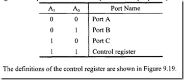
The 8086 configures the three ports by outputting appropriate data to the 8-bit control register. The ports can be decoded by two 8255 input pins A0 and A,, as follows:
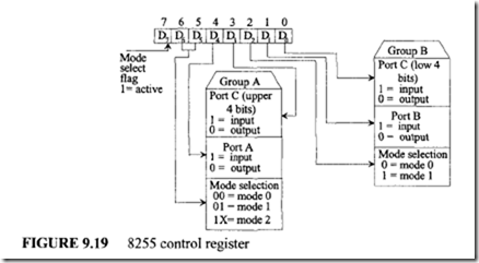
Bit 7 (D7) of the control register must be 1 to send the definitions for bits 0-6 (D0-D6) as shown in the diagram. In this format, bits D0-D6, are divided into two groups: groups A and B. Group A configures all 8 bits of port A and the upper 4 bits of port C; group B defines all 8 bits of port B and the lower 4 bits of port C. All bits in a port can be configured as a parallel input port by writing a 1 at the appropriate bit in the control register by the 8086 OUT instruction, and a 0 in a particular bit position will configure the appropriate port as a parallel output port. Group A has three modes of operation: modes 0, 1, and 2. Group B has two modes: modes 0 and I. Mode 0 for both groups provides simple I/O operation for each of the three ports. No handshaking is required. Mode 1 for both groups is the strobed I/O mode used for transferring I/O data to or from a specified port in conjunction with strobes or handshaking signals. Ports A and B use the pins on port C to generate or accept these handshaking signals. Mode 2 of group A is the strobed bidirectional bus I/O and may be used for communicating with a peripheral device on a single 8-bit data bus for both transmitting and receiving data (bidirectional bus I/O). Handshaking signals are required. Interrupt generation and enable/disable functions are also available.
When D7 = 0, the bit set/reset control word format is used for the control register This format is used to set or reset the output on a pin of port Cor when enabling of the interrupt output signals for handshake data transfer is desired. For example, the 8 bits (OXXXllOO) will clear bit 6 of port C to zero. Note that the control word format can be output to the 8255 control register by using the 8086 OUT instruction. Now, let us define the control word format for mode 0 more precisely by means of a numerical example. Consider that the control word format is 100000102 • With this data in the control register, all 8 bits of Port A are configured as outputs and the 8 bits of port C are also configured as outputs. All 8 bits of port B, however, are defined as inputs. On the other hand, outputting 100110112 into the control register will configure all three 8-bit ports (ports A, B, and C) as inputs.
9.9.4 Important Points To Be Considered for 8086 Interface to Memory and I/O
From the preceding discussions, the following points can be summarized:
1. For ROMs/EPROMs/PPROMs, BHE and A0 are not required as part of chip enable/select decoding.
2. For RAMs and I/O port chips, both BHE and A0 must be used in chip select logic.
3. For ROMs/EPROMs/PPROMs and RAMs, both even and odd chips are required.
However, for I/O chips, an odd-addressed I/O chip, an even-addressed I/O chip, or both can be used, depending on the number of ports required in an application. The 8086 BHE and/or A0 must be used in I/O chip select logic depending on the number and type (odd/even) of I/O chips used.
4. For interfacing ROMs/EPROMs/ PPROMs to the 8086, the same chip select logic must be used for both the even and its corresponding odd memory chip. The same thing applies to RAM and I/O chips except that both BHE and A0 must be
used for RAMs and I/O; however, this is applicable to I/O if both odd and even I/O chips are present in the system.
5. ROMs/EPROMs/PPROMs must be connected in such a way that the 8086 reset vector address FFFF0H is contained in the memory map.
Example 9.19
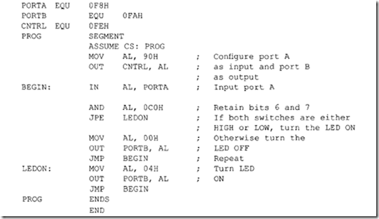
An 8086-8255-2732-6116-based microcomputer is required to drive an LED connected to bit 2 of port B based on two switch inputs connected to bits 6 and 7 of port A. If both switches are either HIGH or LOW, tum the LED ON; otherwise, tum it OFF. Assume a HIGH will tum the LED ON and a LOW will tum it OFF. Write an 8086 assembly language program to accomplish this.
Solution
Example 9.20
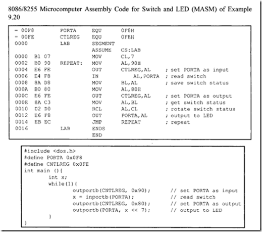
Write an 8086 assembly language program to drive an LED connected to bit 7 of port A based on a switch input at bit 0 of port A. If the switch is HIGH, tum the LED ON; otherwise, tum the LED OFF. Assume an 8086/2732/6116/8255 microcomputer. Also, write a C++ program to accomplish the same task. Compare the 68000 assembly program with the compiled assembly code. Comment on the result.
Solution
The 8086 assembly language program and the C++ program along with the compiled assembly code are shown below. The 8086 assembly program contains 11 instructions whereas the 8086 C++ code generates 16 instructions. This example illustrates that although C++ programming can handle I/O, it generates more codes than assembly language programming. Although programs in C++ are easier to write compared to assembly, the machine code generated by the equivalent assembly language is shorter. Also note that C++ programs are not 100 %portable while the same I/O programs are written using C++ for microprocessors by two different manufactures. This is because of the different hardware configurations (I/O and memory maps) for different manufacturers.
Note that the assembly language program can also be written by rotating bit 0 (switch input) of port A to bit 7 (LED output) of port A only once by using ROR AI, I rather than RCL AL,CL with [CL]=7. The equivalent C++ program will still generate more assembled codes than the assembly language program.
-
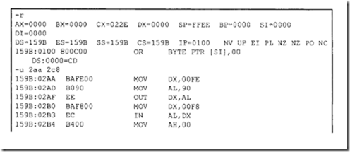
Assembly code generated from C++ code above using Microsoft DEBUG unassembler:
-
8086/8255 Microcomputer C++ program for Switch and LED (C++ Compiler) of Example 9.20
9.10 8086-Based Microcomputer
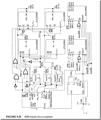
In this section, an 8086 will be interfaced in minimum mode to provide 4K x 16 EPROM, 2K x 16 static RAM, and six 8-bit I/O ports. The 2732 EPROM, 6116 static RAM, and 8255 I/O chips are used for this purpose. Memory and I/O maps are determined. Figure
9.20 shows a hardware schematic for accomplishing this.
The power and ground pins of all chips must be connected together to the power supply’s power and ground pins. The 8086 MN/MX is connected to +5 V for minimum mode (single processor) operation. Linear decoding is used to select both EPROMs and SRAMs. 8086 demultiplexed A 13 = I is used to select 2732s and 8086 demultiplexed A 14 = 0 is used for 6116s. No unused address pin is used for selecting the 8255s because the 8086 M/IO pin distinguishes between memory and I/O.
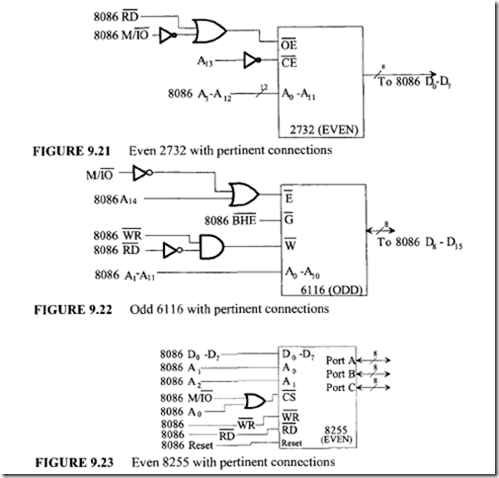
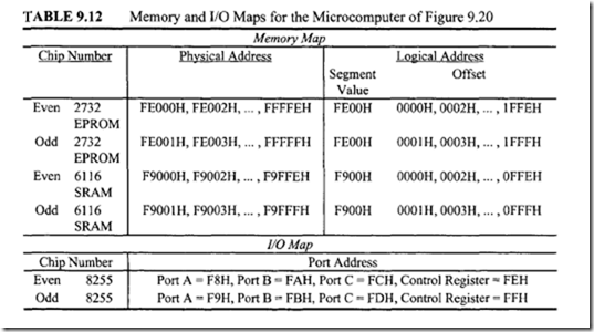
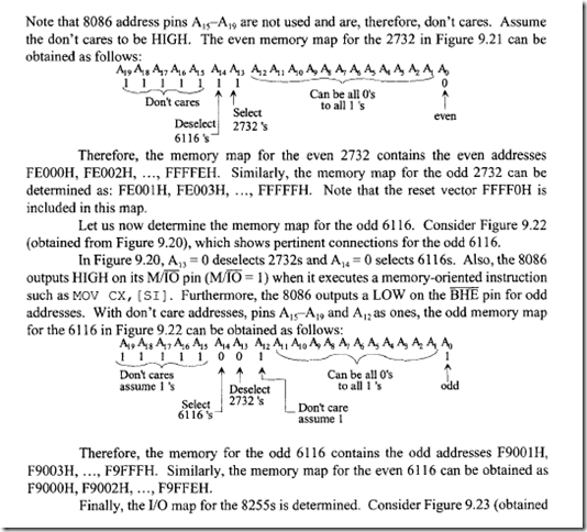
Let us determine the 8086 memory and I/O maps. To determine the memory map for 2732 EPROMs, consider Figure 9.21 (obtained from Figure 9.20), which shows pertinent connections for the even 2732.
In Figure 9.20, M/10 = 1 when the 8086 executes a memory-oriented instruction such as MOV [ BX) , DL to access the memory. Also, in the figure, A 13 = 1 is used to select the EPROMs and A 14 = 1 is used to deselect the RAMs. This is done to include the 8086 reset vector FFFF0 16 in the EPROMs. Therefore, an inverter is used to invert A 13•
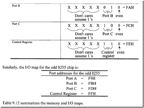
from Figure 9.20), which shows pertinent connections for the even 8255. The 8086 outputs LOW on its M/IO pin (M/IO = 0) when it executes an IN or OUT instruction. The 8086 outputs LOW (A0 = 0) for an even port address. This will produce a LOW on the CS pin of the even 8255. The even 8255 will thus be selected.
Using 8086 A 1 and A2 pins for port addresses, the I/O map for the even 8255 chip can be determined as follows:
