Practical Combinatorial Circuit Implementation
When you are designing your first application that is built from digital electronics, you will probably feel like you have just joined a never-ending role-playing game in which all the other players know more than you do. Later in the book, I will present some ideas on how to read a datasheet and what to look for in it, but for now, I would like to discuss a number of the options that you should be aware of and are thinking about when you first start designing your application.
Using the role-playing game analogy with digital electronics may seem to be facetious, but there are actually a lot of similarities that you should be aware of. First and foremost, each digital electronic chip that you can choose from has a number of characteristics that you will have to be aware of and
Table 6-1 Important characteristics of a digital electronic chip.
|
Characteristic |
Comments |
|
Function |
Gate type, chip function |
|
# Bits |
The number of bits per gate input or number of bits used by the function |
|
# Gates/functions |
What does the chip do and how many are there |
|
Technology |
Electronic standard chip is implemented |
|
Output type |
Gate output type |
|
Dependencies |
Issues to be aware of |
|
Manufacturer |
Who makes the chip/where can it be purchased |
choose from when you are specifying the parts used in your application. When choosing between the parts, it might be a good idea to come up with a card, similar to the cards used in role-playing games to explain the different characters, characteristics and strengths and weaknesses. A sample card for a digital electronic device might look something like Table 6-1.
The ‘‘function’’ of the chip is a brief description of the gates provided by the chip or the digital logic function provided by the chip (such as an adder or a magnitude comparator). At this point in the book, you might feel that it is sufficient to specify a chip for a needed function, but the following characteristics are critical for you to understand that you need to be able to select the right chip for the right application.
When I have presented simple gates, they have all (with the exception of the NOT gate) two inputs. Along with two inputs, there are a number of different inputs for a variety of different types of gates. For example, in standard TTL, you can get NAND gates with two, three, four and eight inputs. Four and eight bit adders as well as different chips with different bit counts are also available. When selecting a chip for an application, you should be cognizant of the bit options that are available to minimize the number of chips required.
The basic TTL chips have four two input gates and six one input gates, but if the number of bits changes, then the number of gates within the chip changes (or the plastic package type and the number of pins changes). As surprising as it seems, many complex functions can have more than one built into the package. Like the number of bits, the number of functions within the chip will help you plan out how many chips you will need in the application.
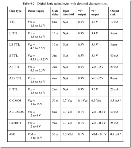
So far in the book, I have really just indicated that there are two types of technology used for standard logic devices. In actuality, there are dozens and in Table 6-2, I have listed the most popular ones with their input, output and operating characteristics. For the different varieties of ‘‘TTL’’, ‘‘C’’, ‘‘AC’’
and ‘‘HC/HCT’’ logic families, the part number starts with ‘‘74’’ and for the ‘‘4000’’ series of CMOS chips, it has a four digit part number, starting with ‘‘4’’. Table 6-2 lists the different aspects of the different types of logic chips that you will want to work with.
The ‘‘output sink’’ currents are specified for a power voltage of 5 volts. If you increase the power supply voltage of the indicated (with a ‘‘*’’) CMOS parts, you will also increase their output current source and sink capabilities considerably.
In Table 6-2, I marked TTL input threshold voltage as ‘‘not applicable’’ (N/A) because, as you know, TTL is current driven rather than voltage driven. You should assume that the current drawn from the TTL ,input is 1 mA for a ‘‘0’’ or ‘‘low’’ input. CMOS logic is voltage driven, so the input voltage threshold specification is an appropriate parameter.
The output current source capability is not specified because many early chips were just able to sink current. This was all that was required for TTL and it allowed external devices, such as LEDs, to be driven from the logic gate’s output without any additional hardware and it simplified the design of the first MOSFET-based logic chips. The asterisk (‘‘*’’) indicates that the sink current specification is for 5 volts power; changing the power supply voltage will change the maximum current sink capability as well.
There are three basic output types: totem pole, open collector and the tri-state driver (which is presented later in this chapter). In cases where multiple outputs are combined, different output types should never be combined due to possible bus contention.
Virtually all of the electrical dependencies that you should be aware of are listed in Table 6-2, but you may have a number of operating dependencies (such as making sure CMOS inputs are tied high or low) or physical design issues that you should be aware of. ‘‘Physical design’’ is the process of designing a printed circuit board with internal connections built into it that have the chips soldered onto it. The primary chip dependencies that you should be aware of when designing a printed circuit board are the location and type of the chip’s pins as well as any heat removal (i.e. heat sinks) requirements that the chip may have.
Finally, you should know who makes the part and where you can purchase it. This point is often overlooked, but you will find many manufacturers that advertise parts that are seemingly designed just for your application. The first problem that you encounter is that your company has a policy of only buying parts that are available from multiple sources or you may discover that the manufacturer is not considered to be reliable and production quantity parts are difficult to come by. For your first designs, it is a good rule to only use parts that are easily obtainable and, ideally, built by multiple sources.
This may make the design operation a bit more difficult and the final product larger than it could have been, but chances are the product will go through manufacturing very smoothly and with few difficult ‘‘hiccups’’.
Race Conditions and Timing Analysis
As you begin to create digital electronic circuits that are more and more complex and run faster and faster, you are going to discover that they are going to stop working or they are going to start working unpredictably. In trying to find the problem, you will probably look at different parts of the circuit, ranging from the power supply to the wiring and maybe rebuilding it several times to see if it is being affected by other electrical devices running near the application. At some point you will give up and build as well as redesign the circuit, only to discover that the problem is still there.
So what’s the problem? Chances are you have encountered a ‘‘race condition’’, which is normally defined as ‘‘A condition in digital electronics where two or more signals do not always arrive in the same order.’’ Personally, I use a slightly different definition for race condition which states that ‘‘A race condition occurs in any digital electronic circuit where the output to input response time changes according to the inputs passed to it.’’ My definition is a bit more specific and should give you some ideas on where to look for the problem.
Simply put, a race condition is a case where an expected event does not occur.
To illustrate the issue, assume that the application consists of a circuit that is designed to respond to an internal value at a specific time. If the digital electronics used to produce this internal value does not always complete within the specified time, what happens in the circuit that uses this value for input? Chances are the circuit will respond incorrectly, resulting in the problem that you are trying to debug.
An example circuit that has the capability of producing a race condition is shown in Fig. 6-1.
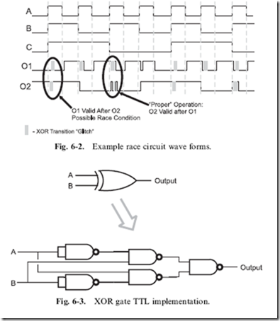
Figure 6-2 is the waveform output of this circuit to a three bit incrementing signal and, in it, I have indicated the output bits (‘‘O1’’ and ‘‘O2’’) and indicated where the operation of the circuit is ‘‘correct’’ (O2 is valid after O1) as well as a possible race condition (when O1 is valid after O2). I have also indicated times, using a shaded block, when both of the XOR inputs are changing and there could be a ‘‘glitch’’ caused by both inputs changing state simultaneously, at which time the output of the XOR gate is unknown.
The glitch produced by the XOR gate is an excellent example of a race condition. As I presented earlier in the book, the XOR gate is typically made up of five NAND gates in the configuration shown in Fig. 6-3. If one input changes, then the output will change state to either ‘‘1’’ or ‘‘0’’ without any glitches, but what happens when the two inputs change state simultaneously?
Quickly thinking about it, you might think that the output doesn’t change state, but consider what happens at the NAND gate level of the XOR gate.
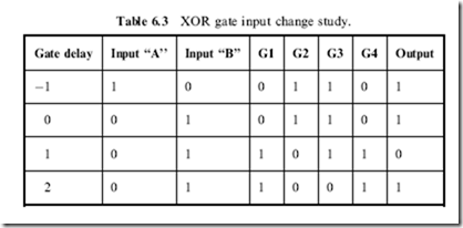
 Table 6-3 lists the NAND gate outputs for the different gates as I’ve marked them in Fig. 6-3. To help illustrate what’s happening, I use ‘‘gate delays’’ as the time increments of this study. In Table 6-3, the initial conditions are one gate delay before the two inputs change value. The inputs change value at gate delay ‘‘0’’.
According to this study, at gate delay 1, the output will be a ‘‘0’’ because
the direct inputs from A and B to G3 and G4 have changed at gate delay 0, but the inverted inputs from G1 and G2 have not. It won’t be until gate delay 2 that the inputs to NAND gates G3 and G4 have stabilized. Thus, the time
from gate delay 1 to gate delay 2 will result in generally unknown logic levels, which are normally characterized by the term ‘‘glitch’’.
Going back to Fig. 6-2, you can probably observe what I mean by the race condition, but I’m sure it seems very subtle. Actually, this is the point that I want to make: race conditions are very subtle and are very difficult to observe. For this section, I spent quite a bit of time with a 74C85 (quad XOR gate), a PIC16F627A (Microchip PIC Microcontroller to produce the ‘‘A’’, ‘‘B’’ and ‘‘C’’ inputs to the circuit) and an oscilloscope trying to capture the events shown in Fig. 6-2. I gave up after about 5 hours of trying to capture the event on the oscilloscope in a way that it would be easily seen.
Race conditions are dependent on part mix, applied voltage and ambient conditions. You may find some sample circuits which never have the problem while others will never seem to work right. Finding the actual event is extremely difficult and only after doing a thorough timing analysis of the circuit will you find the opportunity for a race condition to occur. The prevention for this problem is quite simple – figure out what your worst case gate delay is through the circuit and only sample data after this time
(even add a 10% margin to make sure there is no chance of marginal components causing problems).
Avoiding the opportunity is why chip designers work at making sure multiple outputs are active at the same time for changing inputs. Looking at the ‘‘A’’/‘‘B’’/‘‘C’’ waveform of Fig. 6-2, you might have thought that it is impossible to achieve the signals at precisely the same time, but it is very likely that if a single gate is producing incrementing outputs, the ‘‘edge’’ of each output bit will be precisely aligned with each other and will cause the glitch on the output of the XOR gate.
The process of determining what is the worst case gate delay is the same process I used for finding the ‘‘glitch’’ in the XOR gate and is known as ‘‘timing analysis’’. It is unusual for somebody to work through this analysis by hand as I have done, except for very simple circuits. When timing analysis is done on a commercial product, it is normally done using a logic simulator, which can find the longest delays and report on any problems.


