Feedback and Sequential Circuits
This chapter’s title probably seems like a bit of a misnomer; you are probably wondering what feedback has to do with digital electronics? When I use the term ‘‘feedback’’, I am using it in the most literal sense, past state data are used to maintain current state data. These circuits built from the theory that I am going to provide in this chapter are commonly known as ‘‘memory devices’’. For digital electronic circuits to store information, that information will continually move through the circuit and is used to determine what the future value of the circuit is. Feedback is critical to provide digital electronics with the ability to ‘‘remember’’ previous states and data.
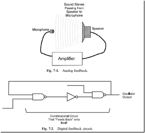
When you first hear the term ‘‘feedback’’, you probably think of an
amplifier with its microphone input brought close to its speaker output (Fig. 7-1). You also probably involuntarily wince at the thought of the term ‘‘feedback’’ because it brings back the memory of the horrible sound the amplifier made when the microphone was too close. This type of feedback
cannot save information; the uncontrolled amplification of the signal distorts and destroys information in a very short order.
When I introduced combinatorial circuits at the start of the book, I noted
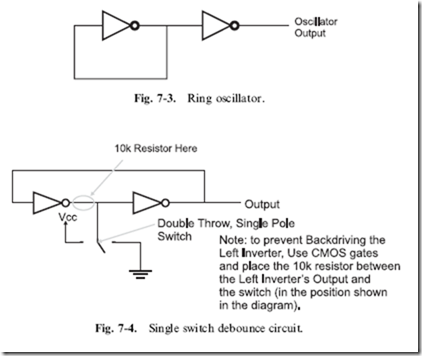
that an important part of combinatorial circuits was that data could only travel in one path; no outputs were passed back to earlier inputs in a logic chain, like the one shown in Fig. 7-2. The reason for specifying that outputs were not to be passed to inputs was to make sure that an inadvertent oscillator, known as a ‘‘ring oscillator’’ (Fig. 7-3), was not created.
You should know that the inverter in Fig. 7-3 is going to invert its input. The problem arises when the input is tied to the output, as it is in this case. When the input is passed to the inverter, it outputs the inverted value, which is then immediately passed back to the input and the gate inverts the value again, and again, and so on.
The ring oscillator is probably the simplest oscillator that you can build and the period of the oscillation runs at literally the speed of the technology’s gate delay times the number of gate delays. If the ring oscillator shown in Fig. 7-3 was built from TTL (which has a gate delay of 8 ns) you would see a ‘‘square wave’’ with a period of 62.5 MHz. One of the functions that ring oscillators perform is the measurement of a logic technology’s gate delay.
Extrapolating from what has been discussed here, you could build a simple memory circuit using the two inverters and a double throw switch, wired as shown in Fig. 7-4. This circuit is used to ‘‘debounce’’ a switch input. As I will discuss in later chapters, when a mechanical switch is thrown, the physical contacts within the switch literally bounce against each other before a hard, stable contact is made. This bouncing can cause quite a bit of grief when you are trying to respond to a single switch movement.
The circuit in Fig. 7-4 will pass a signal continuously between the two
inverters (the output of the two inverters is the same as the input, so there is no chance for a ring oscillator) until the switch comes in contact with a connection that forces the state to change. If the switch was originally at the ground position, the signal coming from the inverter to its left would be a ‘‘0’’. When the switch was moved to the ‘‘Vcc’’ position, the signal going to the inverter to the right would be changed and its output would change.
The beauty of this circuit is that when the switch is in between contacts, the output state of the circuit remains constant.
When the switch is not touching either contact, the two inverters are maintaining the previous bit value and the circuit behaves essentially as a memory device.
There is a downside to the button debounce circuit in Fig. 7-4 and that is when the switch is thrown, it connects the left inverter output to the opposite power supply that it is driving out. This is known as ‘‘backdriving’’ and it should always be avoided.
Backdriving a gate will shorten its life in the best case and could burn it out in very short order. As noted in Fig. 7-4, you should only use CMOS inverters (which are voltage, rather than current controlled) and place the 10 k resistor between the switch and the output of the left inverter. By using this circuit, there will be no chance that the left inverter’s output is tied directly to power or ground (which will be the opposite value that it’s at) and the 10 k resistor will limit the amount of current that is passed. I did not put the resistor into Fig. 7-4 as it is a basic circuit that I have seen in a number of references and I wanted to point out that it does backdrive a gate output and there are ways of avoiding this problem.
The other term used in this chapter’s title, ‘‘sequential circuits’’, is used to
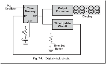
identify the class of digital electronic circuits that have memory devices within them and use their data, along with combinatorial circuits, to produce applications. A digital clock (Fig. 7-5) is an excellent example of a sequential circuit. The data output from the memory circuits of the clock are passed to
combinatorial logic circuits and the outputs of the combinatorial circuits are passed back to the inputs of the ‘‘time memory’’ circuits.
Any time memory circuits, like the ones presented in this chapter, are used in a digital electronics application, the circuit is called a ‘‘sequential circuit’’.
Flip Flops (RS and JK)
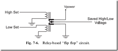
The best analogy I can find for a simple, one bit ‘‘memory device’’ is the two coiled relay of Fig. 7-6. The relay coil does not have a return spring that only one coil pulls against; when the relay’s wiper is placed in a position it stays there. This memory device is set to one of two states, depending on which relay coil was last energized, pulling the wiper contact into connection with it. Once electricity to the coil is stopped, the memory device will stay in this state until the other coil is energized and the wiper is pulled towards it. This device works very similarly to the most basic electronic memory device that you will work with, the ‘‘reset-set’’ (RS) ‘‘flip flop’’.
The term ‘‘flip flop’’ is indicative of the operation of the memory device: it
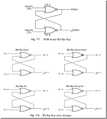
is either ‘‘flipped’’ to one value or ‘‘flopped’’ to another. Where the relay device relies on friction to keep the saved value constant, the electronic memory unit takes advantage of feedback to store the value. Digital feedback can only be one of two values, so its use in circuits probably seems like it is much more limited than that of analog feedback. This is true, except when it is used as a method to store a result in a circuit like the ‘‘NOR flip flop’’, shown in Fig. 7-7. Normally, the two inputs are at low voltage levels, except to change its state, in which case one of the inputs is raised to a high logic level.
If you are looking at this circuit for the first time, then it probably seems like an improbable device, one that will potentially oscillate because if the output value of one gate is passed to the other and that output is passed to
the original, it seems logical that a changing value will loop between the two gates. Fortunately, this is not the case; instead, once a value is placed in this circuit, it will stay there until it is changed or power to the circuit is taken away. Figure 7-8 shows how by raising one pin at a time, the output values of the two NOR gates are changed.
When the ‘‘R’’ and ‘‘S’’ inputs to their respective NOR gates are low, there is only one signal left that will affect the output of the NOR gates and that is output of the other NOR gate. When ‘‘Q’’ is low, then a low voltage will be passed to the other NOR gate. The other NOR gate outputs a high voltage because its other input is low. This high signal is passed to the original
NOR gate and causes it to output a low voltage level, which is passed to the other NOR gate and so on.. . .
The outputs of the flip flop are labeled as ‘‘Q’’ and ‘‘_Q’’. ‘‘Q’’ is the positive output while ‘‘_Q’’ is the negative value of ‘‘Q’’ – exactly the same as if it were passed through an inverter. The underscore character (‘‘_’’) in front of the output label (‘‘Q’’) indicates that the signal is inverted (the same as if an exclamation mark (‘‘!’’) is used for an inverter’s output). When you look at some chip diagrams, you will see some inputs and outputs that have the underscore before or on the line above the pin label.
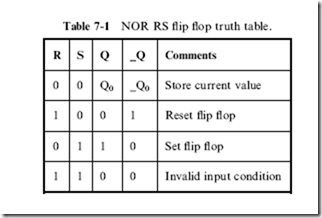
The ‘‘R’’ and ‘‘S’’ input pins of the flip flop are known as the ‘‘reset’’ and ‘‘set’’ pins, respectively. When the ‘‘R’’ input is driven high the ‘‘Q’’ output will be low and when ‘‘S’’ is high the ‘‘Q’’ output will be driven high. These values for ‘‘Q’’ will be saved when ‘‘R’’ and ‘‘S’’ are returned to the normal low voltage levels. ‘‘Q0’’ and ‘‘_Q0’’ are the conventional shorthand to indicate the previous values for the two bits and indicates that the current values of ‘‘Q’’ and ‘‘_Q’’ are the same as the previous values. Truth tables are often used to describe the operation of flip flops and the truth table for the NOR RS flip flop is given in Table 7-1.
In Table 7-1, I have marked that if both ‘‘R’’ and ‘‘S’’ were high, while the outputs are both low, the inputs were invalid. The reason why they are considered invalid is because of what happens when R and S are driven low. If one line is driven slower than the other, then the flip flop will store its state. If both R and S are driven low at exactly the same time (not a trivial feat), then the flip flop will be in a ‘‘metastable’’ state, Q being neither high nor low, but anything that disturbs this balance will cause the flip flop to change to that state. The metastable state, while seemingly useless and undesirable is actually very effective as a ‘‘charge amplifier’’ – it can be used to detect very
small charges in capacitors. This is an important mode of operation that is taken advantage of for DRAM and SDRAM memories.
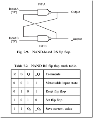
Along with building a flip flop out of NOR gates, you can also build one out of NAND gates (Fig. 7-9). This circuit works similarly to the NOR gate, except that its metastable state occurs when both inputs are low, and the inputs are active at low voltage levels, as I have shown in Table 7-2, which is the NAND RS flip flop’s truth table.
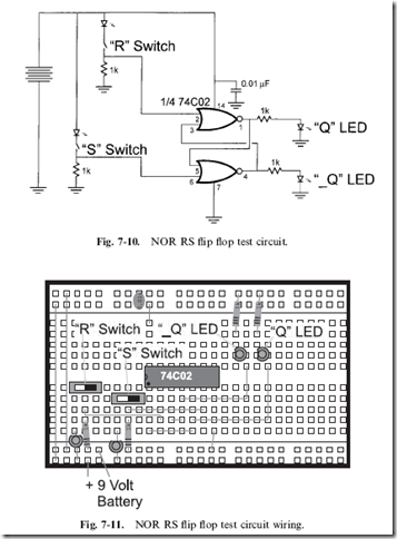
You can build your own NOR RS flip flop, which has its state set by two switches as I show in Fig. 7-10 and is wired according to Fig. 7-11.
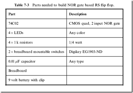
I suggest that you test out the circuit in as many different ways as possible – especially investigating the metastable and post-metastable states. Unless you were to wire the R and S inputs to one switch, you will find it impossible to achieve the metastable state. The parts that are needed to build the RS flip flop are listed in Table 7-3.
Before going on, there is one additional point about flip flops that may not be immediately obvious but will be something that you will have to consider
in your career as a designer of digital electronic devices; when power is removed, the flip flops will lose the bit information contained within them. The term used to describe this phenomena is ‘‘volatility’’; flip flops are considered ‘‘volatile’’ devices. Flash memory (like the flash used in your PC) does not lose its information when power is shut off and is known as ‘‘non-volatile’’ memory.
Edge Triggered Flip Flops
The RS flip flop is useful for many ad hoc types of sequential circuits in which the flip flop state is changed asynchronously (or whenever the appropriate inputs are active). For most advanced sequential circuits (like a micro- processor), the RS flip flop is a challenge to work with and is very rarely used. Instead, most circuits use an ‘‘edge triggered’’ flip flop which only stores a bit when it is required. You will probably discover the edge triggered flip flop (which may also be known as a ‘‘clocked latch’’) to be very useful in your own applications and easier to design with than a simple RS flip flop.
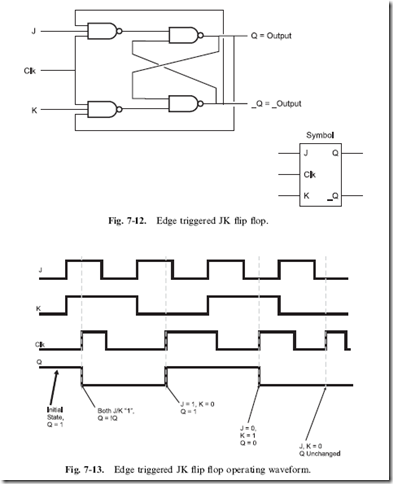
The most basic type of edge triggered flip flop is the ‘‘JK’’ (Fig. 7-12), which provides a similar function to the RS flip flop except that it changes state when the ‘‘clock’’ input is ‘‘rising’’ (changing from ‘‘0’’ to ‘‘1’’), as shown in the waveform diagram of Fig. 7-13.
There are a few points about Fig. 7-13 that should be discussed. I have assumed that in the initial state for this example, the output value ‘‘Q’’ is ‘‘1’’. When the first rising edge of the clock (‘‘Clk’’) is encountered, both J and K are 1, so Q ‘‘toggles’’ or changes state. Next, when the rising edge of the clock is encountered, J is 1 and K ¼ 0, so Q becomes 1 and the opposite is true for the next rising edge. In the final rising edge, both J and K are 0 and the value of Q remains the same. There is no metastable state for the JK flip flop. The operation of the JK flip flop is outlined in Table 7-4.
Just as a small circle on an input or an output of a logic gate indicates that the value is inverted, the clock pin on some chip diagrams is indicated by a small triangle. This convention helps minimize the clutter present in a logic diagram.
The JK flip flop is useful in general digital electronics applications, but it does not provide the necessary function for a computer register. Ideally,
a clocked register’s block diagram is quite simple (Fig. 7-14), consisting of a data line passed to the flip flop along with a ‘‘clock’’ line. While the data line stays constant, the contents of the flip flop doesn’t change. When the clock line goes from high to low, the data is stored in the flip flop – this is known as a ‘‘falling edge clocked flip flop’’ or a ‘‘falling edge clocked register’’ and it is probably the most common type of flip flop that you will work with.
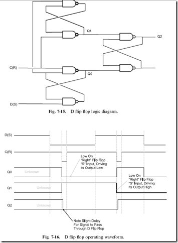
The edge triggered flip flop (Fig. 7-15) is based on the RS flip flop. Instead
of always calling this circuit a ‘‘falling edge triggered flip flop’’ or ‘‘clocked register’’, this circuit is normally known as a ‘‘D flip flop’’. The organization of the flip flops used in this circuit may seem complex, but their operation is actually quite simple: the two ‘‘input’’ flip flops ‘‘condition’’ the clock and data lines and only pass a changing signal when the clock is falling, as I show in Fig. 7-16. To try and make it easier for you to understand, I have marked the outputs of the RS flip flops in Fig. 7-15 and showed the waveforms at these points.
Note that in Fig. 7-16, I have marked the flip flop states before the first clock pulse as being ‘‘unknown’’ (in Fig. 7-14, the initial state was assumed). This is actually a very important point and one that you will have to keep in mind when you are designing your own circuits. You cannot expect a flip flop to be at a specific state unless it is set there by some kind of ‘‘reset’’ circuit (which is discussed in the next section). The output of the edge triggered flip flop stays ‘‘unknown’’ until some value is written in it. If you look at the signals being passed to the right flip flop (Output Q0), you will see that the inputs are unknown until the ‘‘data’’ line becomes low, at which point the two inputs to the right flip flop become high and the ‘‘unknown’’ bit value is stored properly in the flip flop.
The first value written into the D flip flop is ‘‘zero’’, the ‘‘data’’ line’s value for the write is changed before the ‘‘clock’’ line goes negative. When the ‘‘clock’’ line goes low, it forces out a ‘‘1’’ to be passed to the ‘‘right’’ flip flop, keeping it in its current state. The operation of the edge triggered flip flop should become very obvious if you were to build it (it would require two 74C00s).
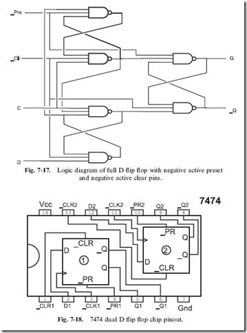
I find the D flip flop to be the flip flop that I build into my circuits most often. It is simple to work with and can interface to microcontrollers and microprocessors very easily. It is, however, quite awkward to wire, especially when you want to work with the ‘‘full circuit’’, which is shown in Fig. 7-17.
This circuit not only has data stored on the rising edge of the clock line but also two other lines ‘‘_Clr’’ and ‘‘_Pre’’ will force the flip flop’s output to a ‘‘0’’ (low voltage) or a ‘‘1’’ (high voltage), respectively, when they are pulled low. This allows for a number of different options for using the D flip flop in your circuit that can allow you to pull off some amazing feats of digital logic.
If you want to experiment with this circuit using two input NANDs (74C00s), I must warn you that it will be quite difficult and complex for you to wire. If you were to use three gates to produce one three input NAND gate, 18 NAND gates would be required to implement the full D flip flop function, which would require four and a half 7400 chips. To demonstrate the operation of the circuit, you could build it out of two 7410 (three, three input NAND gates) or be lazy like I am and just use one 74LS74 (Fig. 7-18) to experiment with the different functions of the full D flip flop.
The 7474 chip consists of two D flip flops with both the ‘‘Q’’ and ‘‘_Q’’ outputs passed to the chip pins. All four inputs shown in Fig. 7-18 (Data and Clock as well as two pins that provide you with the ability to set or reset the state of the flip flop without the use of the data or clock pins) are provided for each of the two flip flops built into the chip. The 7474 is a very versatile chip and can be used for a wide range of applications.
