Boolean Arithmetic Laws
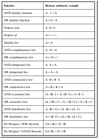
One of the ways of optimizing circuits is look through their output equations and try to find relationships that you can take advantage of using the rules and laws in Table 2-7. These rules should be committed to memory as quickly as possible (or at least written down on a crib sheet) to help you with
Table 2-7 Boolean arithmetic laws and rules.
optimizing logic equations without the need of truth tables or Karnaugh maps. Many of these rules and laws will seem self-evident, but when you are working at optimizing a logic equation in an exam, it is amazing what you will forget or won’t seem that obvious to you.
When I talk about using the laws and rules in Table 2-7 to simplify a logic equation, I normally use the term ‘‘reduce’’ instead of ‘‘optimize’’. The reason for thinking of these operations as a reduction is due to how much the logic equation shrinks as you work through it, trying to find the most efficient sum of products expression.
The two identity functions are used to indicate the conditions where an input value can pass unchanged through an AND or OR gate. The output set, reset and complementary laws are used to output a specific state when a value is passing through an AND or OR gate. The idempotent laws can be summarized by saying that if an input passes through a non-inverting gate, its value is not changed.
The remaining laws – commutative, associative and distributive – and De Morgan’s theorems are not as trivial and are extremely powerful tools when you have a logic equation to optimize. The commutative laws state that the inputs to AND and OR gates can be reversed, which may seem obvious, but when you have a long logic equation that is written in an arbitrary format (not necessarily in sum of product format), you can get confused very easily as to what is happening. It’s useful to have a law like this in your back pocket to change the logic equation into something that you can more easily manipulate.
To demonstrate the operation of these laws, we can go back to some of the logic circuits described in the Karnaugh map examples of the previous section. Looking at Fig. 2-3, the initial sum of products logic equation would be:
Using the AND associative law, I can rewrite this equation with the A term separate from the B and C terms to see if there are any cases where the B and C terms are identical.
 By doing this, I can see that the inside terms of the first and third products are identical. Along with this, I can see that the second and fifth products
are also identical. Using the OR distributive law, I can combine the first and third terms like:
Using the OR complementary law, I know that A OR !A will always be true. This is actually a clear and graphic example of the ‘‘don’t care’’ bit; regardless of the value of this bit, the output will be true so it can be ignored. The partial equation of the two terms reduces to:
The 1 ANDed with !B AND C can be further reduced using the AND identity law (1 AND A equals A):
This can be repeated for the second and fifth terms:
If you go back to the original logic equation, you will see that the fourth term (A · B · C) has not been reduced by combining it with another term. It can actually be paired with the third term (A · !B · C) by rearranging the two terms (using the AND commutative law) so that part of the terms operating on two bits are in common (A · C). Once this is done, the third and fourth terms can be reduced as:
After doing this work, the optimized or reduced sum of product logic equation for this function is
which is identical to what was found using the Karnaugh map.
Looking at the reduced logic equation, you should have noticed that there are two terms that will output a ‘‘1’’ at the same time ((!B · C) and (A · C) with A ¼ 1, B ¼ 0 and C ¼ 1). This is not a problem because the OR gate (even though the symbol that I use is a ‘‘þ’’) will only output a 1, regardless of how many true inputs it has. This was mentioned when the
Karnaugh maps were presented, but I wanted to reinforce that the same issue is present when you are reducing logic equations.
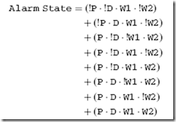
Before moving on, let’s go back to the home alarm logic equation and see if it can be reduced in the same way as the example above. Starting with the sum of products logic equation:
We can bring out the ‘‘P’’ values from the products and look for similarities in the remaining bracketed values and combine them using the associative, distributive, complementary and AND identity laws. I can see that the first and fourth, second and seventh can be combined, resulting in the logic equation:
Bringing ‘‘W1’’ to the forefront allows the combination of the third and fourth and fifth and sixth terms of the logic equation above, resulting in the new equation:
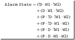
We have eliminated half the terms and, of those remaining, they are 25% smaller. Looking at the new logic equation, we can see that by combining the first and second terms (making ‘‘D’’ a don’t care bit in the process)
and combining the third and fourth terms (‘‘D’’ again is the don’t care bit) we end up with:
which is, again, the logic equation found by optimizing the function using truth tables or Karnaugh maps.
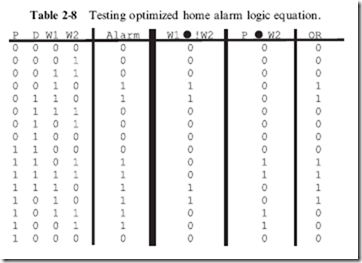
Personally, I tend to optimize logic equations using the Boolean arithmetic laws and rules listed in Table 2-7. Once a reduced sum of products equation has been produced, I then go back and compare its outputs in a truth table with the required outputs. In doing this, I present the values for each product (AND) and the final sum (OR) in separate columns, as shown in Table 2-8.
Optimizing for Technology
If you review the laws in Table 2-7 and correlate them to the text in the previous section, you’ll see that I missed the last two (De Morgan’s theorem). These two laws are not typically used during basic logic equation reduction because they typically involve converting part of an equation into an NAND or NOR gate, which is important when finally implementing a logic function in actual electronics. Another important aspect of optimizing for technology is adding functions out of the leftover gates in your circuit; by looking at how differently a logic circuit could be implemented, you may be able to add functionality to your circuit, without adding any cost to it.
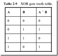
So far in the book, I haven’t discussed the ‘‘Exclusive OR’’ (XOR) gate in a lot of detail, but it is vital for implementing binary adders, as I will show you later in the book. In the first chapter, I presented the XOR gate with the truth table shown in Table 2-9.
You should probably be able to create the logic equation for the XOR
table as:
which does not seem like a very likely candidate for optimization. Similarly, you probably would have a hard time believing that the following logic equation would perform the same function:
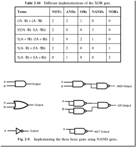
But, using De Morgan’s theorem as well as the other rules and laws from Table 2-7, I can go through the manipulations shown in Table 2-10 to show that they are equal, as well as count out the gates required by intermediate steps to give you a list of different implementations of the XOR gate. Each intermediate step in Table 2-10 is an implementation of the XOR gate that you could implement using the number of gates listed to the right of the terms.
It’s interesting to note that a total of five gates is required for each
implementation – this is not something that you can count on when you are
working at optimizing a circuit.
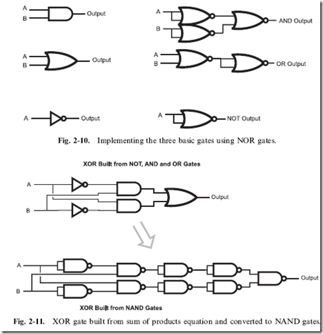
The basic gate used in TTL is the ‘‘NAND’’ gate: this means that the three
basic gates (AND, OR and NOT) are built from multiples of it, as I’ve shown
in Fig. 2-9. The basic gate for CMOS is the NOR gate, and Fig. 2-10 shows
how the three basic gates are implemented for it. The three gate NAND and
NOR equivalencies for the OR and AND gates, respectively, are perfect
examples of De Morgan’s theorem in operation. These implementations
can be checked against De Morgan’s theorem and the rules and laws presented in Table 2-7.
By understanding how gates are implemented in chips, we can now look at how to optimize the gates to provide the fastest possible operation of the logic function. Using the example of the XOR gate, we can graphically show how the gate is implemented using ANDs, ORs and NOTs and how these gates are implemented as NAND gates in TTL chips (Fig. 2-11).
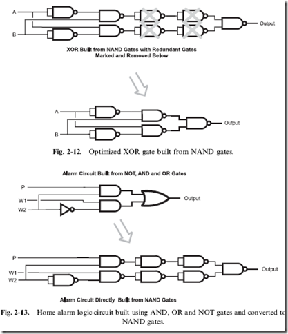
Looking at the bottom logic diagram of Fig. 2-11, you can see that there are two sets of NAND gates wired as inverters together. Going back to Table 2-7, we can see that a doubly inverted signal is the same signal, so we can eliminate these two sets of NOT gates, as shown in Fig. 2-12. The resulting XOR circuit will pass signals through three NAND gates, which
counts as three ‘‘gate delays’’. This is an example of what I call ‘‘technology optimization’’: the logic circuit has been reduced to its bare minimum, taking advantage of the operation of the basic logic gates that make up the technology that it is implemented in.
Before moving on, I want to take one more look at the home alarm circuit that has been discussed throughout this chapter. I made a pretty bold statement at the start of the chapter, saying that it could be reduced to fit into the most basic TTL chip available – let’s see how honest I was being.
The (repeatedly) optimized logic equation for the home alarm system was:
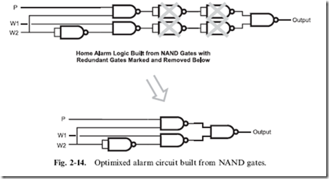
which could be first implemented in two AND, one OR and one NOT gate, as shown in Fig. 2-13 and converted to just NAND gates. You may have noted in Fig. 2-13 the remarkable similarity between the home alarm logic diagram and the XOR logic diagram – as I’ve shown in Fig. 2-14, the logic function reduces to just four NAND gates (one less than the XOR gate built out of NAND gates).
The final home alarm logic function requires four two input NAND gates – which is just what the 7400, the most basic TTL chip, provides. Every TTL chip, except for this one and a derivative revision, has more than four
gates built into them because they provide additional functions requiring multiple NAND gates. I was not exaggerating when I said that the home alarm logic function could be reduced to the most basic TTL chip available. In the next chapter, I will introduce you to the operation of TTL chips that provide the basis for digital electronic logic functions.
Quiz
1. The three parameters that are used to measure the optimization of a digital electronic circuit are:
(a) Cost, speed and complexity
(b) Gate delay, gate count and technology optimization
(c) Gate count, number of gate delays a signal must pass through and technology optimization
(d) Gate count, number of connections a signal must pass through and technology optimization
2. If TTL logic has a gate delay of 8 ns and the signal passing through an XOR gate built from NAND gates has to go through 9 gates and the shortest path is five gate delays, the time required for a signal to pass through the gates is:
(a) 40 ns
(b) 8 ns
(c) indeterminate
(d) 24 ns
3. When writing out a truth table, the inputs should be listed:
(a) Using a ‘‘Gray code’’
(b) Using a ‘‘binary progression’’
(c) In alphabetical order
(d) In order of importance
4. The ‘‘don’t care’’ bit in a truth table is:
(a) Indicated by a ‘‘dc’’ and replaces the common bits in two true sets of inputs
(b) Indicated by an ‘‘x’’ and replaces the common bits in two true sets of inputs
(c) Indicated by a ‘‘dc’’ and replaces the uncommon bits in two true sets of inputs
(d) Indicated by an ‘‘x’’ and replaces the uncommon bits in two true sets of inputs
5. When optimizing a logic function you can expect:
(a) That the number of chips that are required is reduced from the initial design
(b) That the optimized function runs faster than the initial design
(c) Cheaper chips can be used than in the initial design (d) Answers (a) through (c) are all possible and it might not be able to optimize the circuit from the initial sum of products equation
6. Karnaugh maps are:
(a) Tools designed to help you find your way around a digital electronic circuit
(b) A tool that will help you optimize a logic function
(c) The most efficient method of optimizing logic fuctions
(d) Hard to understand but must be used in every logic function design
7. The sum of products logic equation
can be reduced to:
(a) A · C
(b) !A · !B
(c) C · !B
(d) C
8. Which of the following pairs of Boolean arithmetic laws cannot be used together?
(a) Identity and De Morgan’s theorem
(b) Associative and idempotent
(c) Complementary and commutative
(d) All the laws and rules can be used together
9. The NAND equivalent to an AND gate is:
(a) Built from two NAND gates and requires two gate delays for a signal to pass through
(b) Built from three NAND gates and requires two gate delays for a signal to pass through
(c) Built from three NAND gates and requires three gate delays for a signal to pass through
(d) Built from one NAND gate as well as a NOT gate and requires two gate delays for a signal to pass through
10. Technology optimization is defined as:
(a) Designing the circuit which uses the fewest number of chips and signals pass through it as fast as possible
(b) Implementing logic functions to take advantage of the base logic of the logic technology used as well as using any leftover gates
(c) Finding the most efficient digital electronic technology to use for the application
(d) Designing circuitry that dissipates the least amount of heat to perform a desired function
