Programmable DMA Controller (DMAC) 8257
1. Draw the pin diagram of8257.
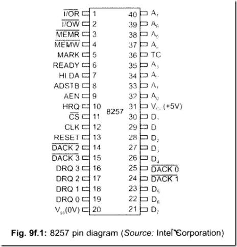
Ans. The following figure gives the pin connection diagram of 8257.
2. Draw the functional block diagram of8257.
Ans. The following figure shows the functional block diagram of the DMAC 8257.
As is apparent from the figure, it consists of eight blocks: data bus buffer, readlw1·ite block, control logic and mode set register, priority resolver and four channel blocks.
3. Describe the general features of 8257. Ans. The general features of 8257 are as follows:
1. It is a 4-channel Direct Memory Access (DMA) interface IC which allows data transfer between memory and up to 4 I/O devices, bypassing CPU.
2. A maximum of 16 KB of data (= 214) can be transferred by this IC sequentially at a time. When a DMA request comes from a peripheral, the DMAC 8257, via its HRQ
(Hold Request) pin (pin number 10, which is an output pin), requests the CPU on its HOLD pin (pin number 39 of CPU 8085). CPU then acknowledges this request via its HLDA (pin 38) pin which goes to HLDA pin (pin 7) of 8257. After this, DMAC generates the required MEMR , MEMW , I/OR , I/OW signals through its 1-4 pins.
3. Initialisation of the DMAC is done under program control for each channel. The parameters which need to be initialised for each channel are starting address, number of bytes of data to be transferred, mode of operation, etc.
4. DMAC can be operated in three modes: (a) DMA Read (reading from memory, writing
into peripheral), (b) DMA Write (writing into memory, reading from peripheral),
(a) DMA verify.
5. Priority for each of the 4 channels can be set in (a) fixed priority, (b) rotating priority.
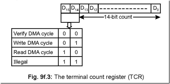
6. A Terminal Count Register exists for each of 4 channels. The number of bytes of data to be transferred is stored in the D13–D0 positions of the 16-bit Terminal Count Register. On completion of data transfer, the Terminal Count (TC) (pin 36, an output pin) goes high.
4. How many I/O devices can 8257 access? Ans. Up to 4 I/O devices can be accessed by 8257.
5. What is the maximum value of KB of data that 8257 can transfer? Ans. 8257 can transfer a maximum of 16 KB (16,384 = 214) of data.
6. What are the modes of operation of 8257? Ans. 8257 can be operated in three modes. These are:
z DMA read
z DMA write and
z DMA verify
7. Comment on priority when 8257 services the external I/Os for data transfer.
Ans. Priorities, to service the external interrupts, can be
z fixed priority.
z rotating priority.
In the Mode Set Register (it is also called control register) of 8257, D4 bit corresponds to ‘enable Rotating Priority’ bit.
If this bit is not set, then CH–0 is assigned highest priority and CH–3 lowest priority—this is by default. If D4 is set to ‘1’, the channel that has just been serviced is allocated the lowest priority. The DMA operation always assigns highest priority to CH–0.
If more than one channels are enabled, and they all place the request for DMA transfer, consecutive DMA cycles service different channels, beginning with CH–0.
8. What are the registers available with each channel of 8257?
Ans. The registers which are available with each channel of 8257 are:
z An Address Register (16-bit)
z A Terminal Count Register (TCR) (16-bit)
9. How the 8257 is initialised?
Ans. The 8257 is initialised by the CPU
(a) by loading the starting address of a DMA block for an I/O device in the 16-bit address
register.
(b) by loading D13 – D0 bits i.e., lower 14-bits of Terminal Count Register (TCR) with the number of bytes of data to be transferred.
(c) by loading D15 and D14 of TCR appropriately to set the mode of operation of 8257.
(d) by loading the Mode Set Register appropriately.
10. When does the status of pin 36 (TC = Terminal Count) of 8257 go high?
Ans. Pin 36 of 8257, which is the TC pin (an output pin, active high type) is raised high (‘1’ state) when the contents of TCR of the selected channel become zero.
11. What are meant by an enabled and a disabled peripheral?
Ans. The peripherals which are granted DMA transfer are called enabled peripherals and the
ones who are denied DMA transfer are called disabled peripherals. The above is done by Mode Set Register.
12. What are the jobs that are performed by 8257 sequentially, when it receives a request from an enabled peripheral?
Ans. 8257 does the following jobs sequentially, when it receives a request from an enabled peripheral:
(i) Gains control of the system buses, once the HOLD signal issued by 8257, is acknowledged by 8085.
(ii) 8257 sends an acknowledgement signal to the peripheral which is currently having the highest priority.
(iii) The lower 8-bits of the memory address are put out as A0 – A7 pins. These are connected to the A0 – A7 lines of the system bus. The most significant 8-bits of the memory address are put via the data bus lines D0 – D7. These are latched by 8212 latch which places them on the system address bus A8 – A15.
(iv) I/O read/write and memory read/write signals are generated.
13. Which pin of 8257 acts in a similar fashion as the ALE (address latch enable) pin of 8085? Elaborate.
Ans. Pin 8 which is ADSTB (address strobe) is an active high output pin and functions in the same manner as the ALE pin of 8085.
At the beginning of each DMA cycle, 8257 puts the most significant byte of the DMA address register on its D0 – D7 pins. These are latched by 8212 latch using the ADSTB strobe pulse of 8257. Thus at the end of this cycle, the D0 – D7 pins of 8257 can be used for data transfer purpose.
14. Where the number of bytes of data, to be transferred by DMA mode, are stored? Ans. The number of bytes of data to be transferred by DMA mode are stored in D0 – D13 bits
of Terminal Count Register (TCR). They are loaded with a value which is the required number of DMA cycles minus one.
As shown, the two bits D15 and D14 together are loaded to set the mode of operation for that channel—like DMA write or read cycle, etc.
15. With regard to data transfer, how many classes of DMA are possible? Ans. With regard to data transfer under DMA control, two classes are possible:
(i) Sequential DMA: In this, the DMA controller reads a data byte from memory and then writes the same into I/O or vice-versa. For each of these read or write operations, 2 to 4 CLK cycles are required.
![]() (ii) Simultaneous DMA: It is the fastest transfer process. Here Read and Write operations are performed at the same time. Thus both MEMR and lOW (or lOR and MEMW) are active at the same time. Thus a speed improvement oftwice the sequential DMA class is possible in this case.
(ii) Simultaneous DMA: It is the fastest transfer process. Here Read and Write operations are performed at the same time. Thus both MEMR and lOW (or lOR and MEMW) are active at the same time. Thus a speed improvement oftwice the sequential DMA class is possible in this case.
When bulk data is to be transferred, (i) is used while (ii) is used for moderate data transfer.
16. Why DMA mode of data transfer scheme is the fastest?
Ans. In normal data transfer schemes, a data coming from an I/0 is first taken to ACC of the CPU and then stored in memory.
But in DMA scheme, straightway data exchange takes place between memory and I/0, bypassing the ACC of CPU. Since ACC of CPU does not take part (it is absent) in DMA mode of data transfer scheme, thus this mode is fastest.
17. What are the basic building blocks of 8257? Ans. The basic building blocks are as follows:
DMA channels, Data bus buffer, Read/Write block ( I/OW , I/OR , CS, Reset, CLK, Ao – A3), control logic block (HRQ, HLDA, A4 – A7, MEMW, MEMR , Ready, ADSTB, AEN, TC, MARK) and Mode Set Register.
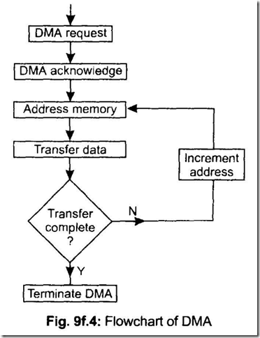
18. Draw the basic flowchart of a DMA mode of data transfer scheme. Ans. The flowchart will be, as shown below:
19. What is meant by a DMA cycle?
Ans. A DMA cycle indicates the transfer of a byte.
20. Through which pin a peripheral requests the 8257 for data transfer and through which pin the peripheral gets back the acknowledgement.
Ans. A peripheral requests for data transfer to 8257 via DRQ (DRQ 0 – DRQ 3) pin and it gets back the acknowledgement via DACK ( DACK 0 – DACK 3 ) pin.
21. What determines the master or slave action of a DMA controller.
Ans. When the mP is in control of its buses (address bus, data bus and control bus), it acts as master and DMA controller acts as the slave. When DMA controller takes control of the buses, it becomes the master and mP becomes the slave.
22. What are the functions of Mode Set Register of 8257 DMA controller? Ans. The functions of the Mode Set Register are as follows:
(i) To enable/disable a channel or channels.
(ii) To configure 8257 in the following four categories: Auto Load, TC Stop, Extended
Write, Rotating Priority.
23. When DMA is undertaken, with whom the peripheral is synchronised?
Ans. When DMA is in progress, the peripheral is synchronised to the main memory, not the microprocessor.
24. When the DMA request line (i.e., HOLD pin of microprocessor) is sampled? Ans. It is sampled at the end of each machine cycle and not instruction cycle.
Thus the response time for a DMA request is a maximum of one machine cycle plus
one T state. For 8085 or Z–80 microprocessors the worst case scenario, i.e., maximum
time is 7 (seven) T states.
25. When a non-maskable interrupt is not going to be recognised by a micro- computer system?
Ans. No interrupts—either maskable or non-maskable—will be recognised during a DMA request.
26. In how many modes DMA transfer is possible?
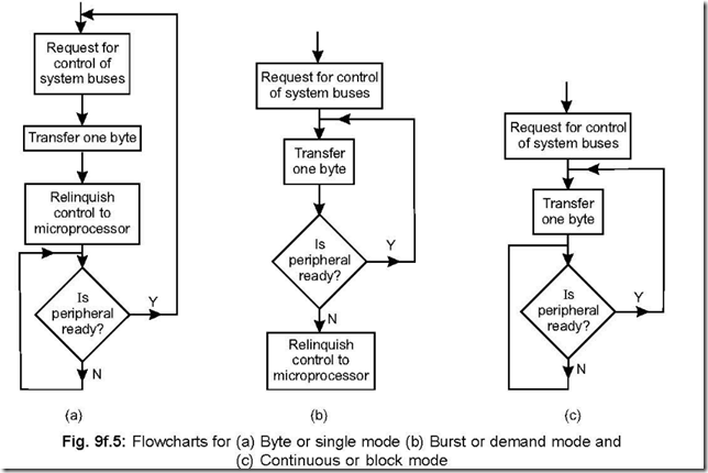
Ans. There are three modes. These are: (a) Byte or Single mode, (b) Burst or Demand mode,
(c) Continuous or Block mode
In byte or single mode, after transferring one byte of data, the bus control is relinquished and handed over to microprocessor.
In burst or demand mode, data is transferred till the time the peripheral is ‘ready’. After this the bus control is handed over to microprocessor.
The third method, i.e., continuous or block mode, is identical to the earlier one, but the bus control is not relinquished until the entire block of data has been transferred.
27. Which particular register is responsible for enabling (or disabling) a particular channel?
Ans. It is the shift mode set register which is responsible for enabling (or disabling) of a particular channel (CH0 to CH3). The mode set register is defined as:
For example, if channel 1 (CH–1) is to be selected (enabled), along with TC stop option facility, then the mode set register, as per above, should have the following content:
0 1 0 0 | 0 0 1 0 = 42 H
28. How the port addresses of the registers in 8257 are done?
Ans. The port addresses of each register in 8257 are determined by the four address lines A3–A0. The port assignments for mode register, CH–1 DMA register and CH–1 count register are given below:
It is assumed that CS signal is connected to address line A7 via an inverter and A6 – A4 are all at logic level 0.
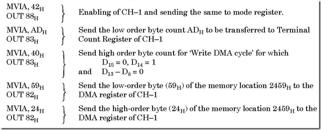
29. Write a program to transfer ADH bytes of data from a peripheral to memory, the memory address starting from 2459H. Data to be inputed via CH–1.
30. Which particular pin of 8257 is used to convert it into ‘master’ mode and MPU in ‘slave’ mode?
Ans. AEN (Address enable) pin of 8257 is utilised to convert it into ‘master’ mode and at the same time translate MPU into ‘slave’ mode.
31. Which particular pin of 8257 is used to interface it with a slow memory?
Ans. ‘READY’ pin of 8257 is used for the purpose. When the memory becomes ready, it sends a high signal which is connected to the ‘READY’ pin of 8257.
32. When 8267 is programmed to have fixed priority, which channel will have the lowest priority?
Ans. It is the CH-3 which will have lowest priority.
33. When data is transferred from memory to an 110, which two of the four signals 1/0R, 1/0W, MEMR, MEMW of8257 become active?
Ans. The signals which become active are MEMR and I!OW. These two signals become active low.
34. What is the function of ‘MARK’ output pin of 8257?
Ans. When this (MARK) output pin goes high, it informs the concerned VO device that the current DMA cycle is the 128th cycle since the previous MARK output.
35. Explain the Auto Load Option of the Mode Set Register of 8257.
Ans. Bit D7 is the ‘Auto Load Option’ bit of Mode Set Register 8257. It is enabled when D7
is set.
This ‘Auto Load Option’ facility is used, i.e., D7 bit of mode set register is set ( = ‘1’) when some DMA operation is repeatedly desired-like the sending of data to a CRT monitor. This is called repetitive or chained DMA operation and utilises CH-2 and CH-3.
36. What does ‘TC stop’ option do when it is set?
Ans. It is the D6 pin of mode set register. When it is set, a channel is automatically disabled when the Terminal Count output goes high. If DMA operation is to be continued or else if another operation is to begin, the channel must be enabled by a fresh Mode Set Operation in the Mode Set Register.
37. Describe the status word register of 8257.
Ans.
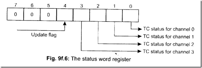
The Status Word Register of 8257 is shown in Fig. 9f.6. It can be read to know the status of the terminal counts of the four channels CHO-CH3. Bit 4 corresponds to the update flag.
Any of the four bits—bit 0 to bit 3 of the status word register is set when the terminal count output corresponding to that channel goes high. When the status word is read, the TC status bits (bits 0 to 3) are cleared.
The update flag is cleared in the following cases:
z When 8257 is reset
z When ‘Auto Load’ option in the ‘Mode Set Register’ is reset.
z When it automatically goes low on the completion of update cycle.
The update flag is not affected when a status read operation is undertaken.
38. Indicate the lengths of the different registers within DMAC 8257.
Ans. 8257 has four channels. Each of these four channels has two 16-bit registers—Address Register and Terminal Count Register.
Again 8257 has two 8-bit registers—a Mode Set Register and a Status Register.
39. Describe the functions of the pins D0 – D7 (pins 21–23, 26–30).
Ans. The functions played by D0 – D7 bits are different for the following two cases: when 8257 is a slave, and when 8257 is a master.
In the ‘slave’ mode of 8257, D0 – D7 pins act as input pins. Eight bits of data at a time for the Address Register or Terminal Count Register (both 16-bits), (for a particular channel) or eight bits of data for the 8-bit Mode Set Register are received through these pins. The CPU can also read eight bits of data at a time from the Address or Terminal Count Registers or from the Status Register.
In the ‘master’ mode of 8257, the DMAC puts out the eight most significant bits of the DMA Address Register (for a particular channel), at the beginning of each DMA cycle, through D0 – D7. These are latched by 8212 latch and these latched values are put out on A8 – A15 of the system address bus. Once this operation is over, D0 – D7 pins are released so that through these pins memory data transfer can be executed for the remainder of the DMA cycle.
40. Discuss the functions of the pins A0 – A3.
Ans. Two different functions are played by these pins for the two cases when 8257 acts as the master or else as a slave.
In the master mode of 8257, these four pins A0 – A3 act as output pins. 8257 puts out the four least significant bits of the DMA Address Register on these four pins.
In the slave mode of 8257, while accessing the Mode Set Register or Status Word Register, the pins A2 A1 A0 must all be ‘0’s, while A3 = 1. Again while mode set operation is done (This is a write only operation), the status of I OW and I OR pins would be 0, 1 while for status word (this is a read only operation), the status of the above two pins would be 1, 0 respectively.
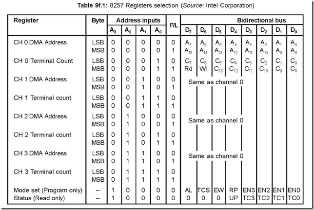
41. Explain, in detail how the Address Registers and Terminal Count Registers for each of CH0–CH3 are selected as also the Mode Set Register and Status Word Register.
Ans. The four Address Registers and four Terminal Count Registers of Channels CH0–CH3 can be accessed only if A3 = 0. For Mode Set Register and Word Register accessing, A3= 1.
For individual channel selection, bits A2 A1 are used. With 00, 01, 10, 11 values for A2 A1 select channels CH0, CH1, CH2 and CH3 respectively, while the status of bit A0 distinguishes between channel and Terminal Count Register. If A0 = 0, any of the channels would be selected and if A0 = 1 then Terminal Count Register would be selected.
The channel registers (Address Register or Terminal Count Register) of each channel are 16-bits each. Thus two operations must be performed on a channel register—one for the lower byte and the other for the upper byte to access it fully—be it reading or writing operation. This distinction between the two halves of a channel are done by a special internal First/Last F/F (F/L F/F). This F/F toggles at the completion of each READ/ WRITE operation. This F/L F/F assumes a ‘0’ state for LSB and ‘1’ for MSB accessing of a channel register.
A channel register, while being accessed, must be accessed fully—i.e., both LSB and MSB of the channel should be accessed. Therefore, before programming of a channel being initiated, the system interrupts must be disabled, otherwise an interrupt occurring after the first half of channel accessing will prevent the second half of the same channel from being accessed.
The F/L F/F is reset when 8257 gets a Reset input or whenever the Mode Set Register is programmed.
The following table shows in details how both the registers in each channel (CH0–CH3), as also the Mode Set Register and Status Word can be selected, so that they can be programmed accordingly.
A0–A15: DMA starting address, C0–C13: Terminal Count Value (N–1), Rd and Wr: DMA verify (00), Write (01) or Read (10) Cycle selection, AL: AUTO Load, TCS: TC STOP, EW: Extended write, RP: Rotating priority, EN3–EN0: Channel enable mask, UP: Update Flag, TC3–TC0: Terminal count status bits.
42. What happens to Mode Set Register when a ‘resetting’ of the system is done?
Ans. When the system receives a ‘reset’, the mode set register is automatically cleared. It disables all the four DMA channels and inhibiting all options.
43. Compare data transfer rate of 8237 DMA and a 2 MHz 8080.
Ans. For the 8237 DMA, the data transfer rate between memory and I/O port is of the order of 1.6 MB/second while it is around 33,000 bytes/second using polling.
