Introduction
In this chapter a hardware configuration for an 805 I microcontroller, which will be used for all of the example applications in Chapters 8 and 9, is defined. Programs that check the initial prototype of the design (debugging programs) are given in this chapter, followed by several common subroutines that can be used by programs in succeeding chapters.
The design of the microcontroller begins with an identified need and a blank piece of
paper or computer screen. The evolution of the microcontroller follows these steps:
1. Define a specification.
2. Design a microcontroller system to this specification.
3. Write programs that will assist in checking the design.
4. Write several common subroutines and test them. L00
The most important step is the first one. If the application is for high-volume production (greater than 10000 units). then the task must be very carefully analyzed. A precise or "tight" specification is evolved for what will become a major investment in factory programmed parts. As the volume goes down for any particular application, the specifications become more general as the designers attempt to write a specification that might fit a wider range of applications.
The list leaves out a few real-world steps, most notably the redesign of the microcontroller after it is discovered that the application has grown beyond the original specification or, as is more common, the application was not well underst00d in the beginning. Experienced designers learn to add a litT1e "fat" to the specification in anticipation of the inexorable need for "one more bit of I/O and one more kilobyte of memory."
A Microcontroller Specification
A typical ouT1ine for a microcontroller design might read as follows:
"A requirement exists for an intelligent controller for real-time control and data monitoring applications. The controller is part of a networked system of identical units that are connected to a host computer through a serial data link. The controller is to be produced in low volumes, typically less than one thousand units for any particular application, and it must be low cost."
The 805l family is chosen for the following reasons:
Low part cost
Multiple vendors
Available in NMOS and CMOS technologies
Software t00ls available and inexpensive
High-level language compilers available
The first three items are very important from a production cost standpoint. The software aids available reduce first costs and enable projects to be completed in a timely manner.
The low-volume production requirement and the need for changing the program to fit particular applications establish the necessity of using external EPROM to hold the application program. In turn, ports o (AD0-AD7) and 2 (AS-Al5) must be used for interfacing to the external ROM and will not be available for I/O.
Because one possible use of the controller will be to gather data, RAM beyond that available internally may be needed. External RAM is added for this eventuality. The immediate consequence of this decision is that port 3 bits 6 (͞W͞R) and 7 (͞R͞D) are needed for the external RAM and are not available for I/O. External memory uses the 2S-pin standard configuration, which enables memories as large as 64K to be inserted in the memory sockets.
Commercially available EPROM parts that double in size beginning at 2K bytes can be purchased. The minimum EPROM size selected is SK and the maximum size is 64K. These choices reflect the part sizes that are most readily available from vendors and parts that are now beginning to enter high-volume production.
Static RAM parts are available in 2K, SK, and 32K byte sizes; again. the RAM sizes are chosen to be SK or 32K to reflect commercial realities. The various memory sizes can be incorporated by including jumpers for the additional address lines needed by larger memories and pull up resistors to enable alternate pin uses on smaller memories.
The serial data needs can be handLED by the internal serial port circuitry. once again, two more I/O pins of port 3 are used: bits 3.0 (RXD) and 3.l (TXD). We are left with all of port l for general-purpose I/O .and port 3 pins 2-5 for general-purpose I/O. or for external interrupts and timing inputs.
Note that rapid loss of I/O. capability occurs as the alternate port functions are used and should be expected unless volumes are high enough to justify factory-programmed parts.
The handicap is not as great as it appears, however; two methods exist that are commonly used to expand the I/O. capability of any computer application: port I/O. and memorymapped I/O.
Finally, we select a l6 megahertz crystal to take advantage of the latest high-speed devices available, and the specification is complete. To summarize, we have
80C3 l – l (ROM less) microcontroller
64K bytes of external EPROM
32K bytes of external RAM
8 general-purpose I/O lines
4 general-purpose or programmable I/O lines
1 full-duplex serial port
16 megahertz crystal clock
Now that the specification is complete, the design can be done.
A Microcontroller Design
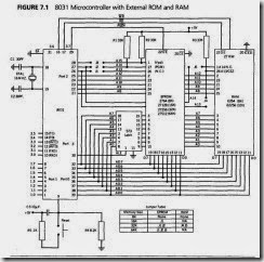
The final design, shown in Figure 7. l, is based on the external memory circuit found in Chapter 2. Any I/O circuitry needed for a particular application will be added to the basic design as required. A design may be done in several ways; the choices made for this design are constrained by cost and the desire for flexibility.
External Memory and Memory Space Decoding
External memory is added by using port o as a data and low-order address bus, and port 2 as a high-order address bus. The data and low addresses are time multiplexed on port o. An external 373 type address latch is connected to port 0 to store the low address byte whenever external memory is accessed. The low-order address is gated into the transparent latch by the ALE pulse from the 805l . Port 0then becomes a bidirectional data bus during the read or write phase of a machine cycle.
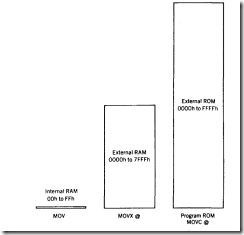
RAM and ROM are addressed by entirely different control lines f ROM the 8051: PSEN for the ROM and WR or RD for the RAM. The result is that each occupies one of two parallel 64 kilobyte address spaces. The decoding problem becomes one of simply adding suitable jumpers and pullup resistors so that the user can insert the memory capacity needed. Jumpers are inserted so that the correct address line reaches the memory pin or the pin is pulLED high as required by the memory used. The jumper table in Figure 7. I for the EPROM and RAM memories that can be inserted in the memory sockets shows the jumper configuration. Figure 7 .2 graphically demonstrates the relative sizes of the internal and external memories available to the programmer.
Reset and Clock Circuits
The 8051 uses an active high reset pin. The reset input must go high for two machine cycles when power is first applied and then sink low. The simple RC circuit used here will supply system voltage (Vee) to the reset pin until the capacitor begins to charge. At a threshold of about 2.5 V, the reset input reaches a low level, and the system begins to run. Internal reset circuitry has hysteresis necessitated by the slow fall time of the RC circuit.
The addition of a reset button enables the user to reset the system without having to turn power off and on.
The clock circuit of Chapter 2 is added, and the design is finished.
Expanding I/O
Ports l and 3 can be used to form small control and bidirectional data buses. The data buses can interface with additional external circuits to expand I/O up to any practical number of lines.
FIGURE 7.2 8o3l Memory Sizes
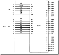
There are many popular families of programmable port chips. The one chosen here is the popular 8255 programmable interface adaptor, which is available f ROM a number of vendors. Details on the full capabilities of the 8255 are given in Appendix D. The 8255 has an internal mode register to which control words are written by the host computer. These control words determine the actions of the 8255 ports, named A, B, and C, enabling them to act as input ports, output ports, or some combination of both.
Figure 7 .3 shows a circuit that adds an 8255 port expansion chip to the design. The number of ports is now three 8-bit ports for the system. The penalty paid for expanding I/O in this manner is a reduction in speed that occurs due to the overhead time needed to write control bits to ports I and 3 before the resulting I/O lines selected can be accessed. The advantage of using I/O port expansion is that the entire range of 8051 instructions can be used to access the added ports via ports I and 3.
Memory-Mapped I/O
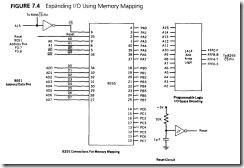
The same programmable chip used for port expansion can also be added to the RAM memory space of the design, as shown in Figure 7 .4. The present design uses only 32K of
the permitted 64K of RAM address space; the upper 32K is vacant. The port chip can be addressed any time Al5 is high (8000h or above), and the 32K RAM can be addressed whenever A l5 is low (7FFFh and below). This decoding scheme requires only the addition of an inverter to decode the memory space for RAM and I/O.
Should more RAM be added to the design, a comprehensive memory-decoding scheme will require the use of a programmable array-type decoder to reserve some portion of memory space for the I/O port chips. Figure 7.4 shows a design that permits the addition of three memory-mapped port chips at addresses FFFoh-FFF3h, FFF4h-FFF7h, FFF8h-FFFBh. and FFFCh- FF
FFh. RAM is addressable from 0000h to FFEFh.
Memory-mapped I/O has the advantage of not using any of the 8051 ports. Disadvantages include the loss of memory space for RAM that is used by the I/O address space, or the addition of memory decoding chips in order to limit the RAM address space loss. Programming overhead is about the same as for port I/O because only the cumbersome MOVX instruction may be used to access the memory-mapped I/O.
For both types of I/O expansion, the cost of the system begins to mount. At some point, a conventional microprocessor, with a rich set of I/O and memory instructions. may become a more economical choice.
Part Speed
one consideration, that does not appear on the design drawings, is the selection of parts that will work at the system speeds determined by the crystal frequency. All memory parts are priced according to the nanosecond of access time. The longer the access time (the time it takes for a byte of data to be read or written from or to the device after the address is valid), the cheaper the part. For our design, Figure 7.4 shows the timing involved in reading data from the ROM and reading and writing data to the RAM. These times are totally determined by the selection of the crystal frequency, and the designer must ch00se memory parts that are fast enough to keep up with the microcontroller at the chosen frequency. For our example, EPROMS with maximum access times of l5o ns and RAM with access times of 400 ns must be used. These access times are representative of standard commercial types currenT1y available at the low end of the cost spectrum. These times are worst-case times; actual access times are at least 3o percent longer.
other parts, such as the ‘373 type latch can be any family from lSTT1 to HCMoS.
The speeds of these parts far exceed the speed of the 8051 .
Production Concerns
The design omits many features that would be incorporated by a design-manufacturing team. Chief among these are the inclusion of test-points, LED indicators, and other items that should he added to enhance manufacturing and field service of the microcontroller.
These concerns are well beyond the scope of this b00k, but the wise designer always ensures that the legitimate concerns of the technical, manufacturing, and service departments are addressed.
Testing the Design
once the hardware has been assemb LED, it is necessary to verify that the design is correct and that the prototype is built to the design drawing. This verification of the design is done by running several small programs, beginning with the most basic program and building on the demonstrated success of each.
Crystal Test
The initial test is to ensure that both the crystal and the reset circuit are working. The 8051 is inserted in the circuit, and the ALE pulse is checked with an oscilloscope to verify that the ALE frequency is I /6 of the crystal frequency. Next, the reset button is pushed, and all ports are checked to see that they are in the high (input) state.
ROM Test
The most fundamental program test is to ensure that the microcontroller can fetch and execute programs from the EPROM. Code byte fetching can be tested by verifying that each address line of the ROM is properly wired by using a series of repeated jump instructions that exercise all of the address lines. The test used here will jump to addresses that are a power of two. only one address line will be high, and all of the rest will be low. The address pattern tests for proper wiring of each address line and also checks for shorts between any two lines.
If the test is successful, the program stops at the highest possible ROM address. The address bus can then be checked with a logic probe to verify that the highest address has been reached. Correct operation is indicated by the highest order address bus bit, which will appear constant. If not, the probe will blink indicating random program fetches.
The test is run by inserting the ‘373 latch, the programmed 64K EPROM, inserting jumpers I – 3 and resetting the 8051 . The test can be stopped at any address by jumping to that address, as is done in the last statement in the following ROM test program:
|
ADDRESS |
MNEMONIC |
COMMENT |
||
|
.org 0000h |
;start at the bottom of ROM |
|||
|
begin: |
l jmp add2 |
;test address lines A0 and Al |
||
|
.org 0004h |
;next jump at address 0004h (A2) |
|||
|
add2: |
1jmp add3 |
;test address line A2 |
||
|
.org 0008h |
;next jump at address 0008h (A3) |
|||
|
add3: |
1jmp add4 |
;test address line A3 |
||
|
.org 0010h |
;next jump at address 0010h (A4) |
|||
|
add4: |
1jmp add5 |
;test address line A4 |
||
|
.org 0020h |
;next jump at address 0020h (A5) |
|||
|
add5: |
1jmp add5 |
;test address line A5 |
||
|
.org 0040h |
;next jump at address 0040h (AG) |
|||
|
Add6: |
1jmp add7 |
;test address line AG |
||
|
.org 0080h |
;next jump at address 0080h (A7) |
|||
|
Add7: |
1jmp add8 |
;test address line A7 |
||
|
.erg 0100h |
;next jump at address 0100h (AB) |
|||
|
add8: |
1jmp add9 |
;test address line A8 |
||
|
.erg 0200h |
;next jump at address 0200 (A9) |
|||
|
add9: |
1jmp addl0 |
;test address line A9 |
||
|
.erg 0400h |
;next jump at address 0400h (Alo) |
|||
|
Add10: |
1jmp add11 |
;test address line Al0 |
||
|
.erg 0800h |
;next jump at address 0800h (All) |
|||
|
Add11: |
1jmp addl2 |
;test address line All |
||
|
. erg 1000h |
;next jump at address 1000h (Al2) |
|||
|
Add12: |
1jmp addl3 |
;test address line Al2 |
||
|
.erg 2000h |
;next jump at address 2000h (Al3) |
|||
|
addl3: |
1jmp addl4 |
;test address line Al3 |
||
|
.erg 4000h |
;last jump at address 4000h (Al4) |
|||
|
addl4: |
1jmp addl5 |
;test address line Al4 |
||
|
.erg 8000h |
;test address line Al5 and remain here |
|||
|
addl5: |
. 1jmp addl5 |
;jump here in a l00p |
||
|
.end |
;assembler use |
|||
|
;This address, Al5, will remain latched while A2-Al4 will |
||||
|
;remain low. Ao and Al will vary as the bytes of the jump |
||||
|
;instruction are fetched. |
||||
Inspection of the listing for this program in Figure 7.5 shows that all the address lines are exercised.
RAM Test
once sure of the ability of the microcontroller to execute code, the RAM can be checked. A common test is to write a so-CALLED checkerboard pattern to RAM-that is, an alternating pattern of 1 and o in memory. Writing bytes of 55h or AAh will generate such a pattern.
The next program writes this pattern to external RAM, then reads the pattern back and checks each byte read back against the byte that was written. If a check fails, then the address where the failure occurred is in the DPTR register. Port l and the free bits of port 3 can then be used to indicate the contents of DPTR.
There are l4 bits available using these ports (the serial port is not in use now, so bits 3.o and 3.l are free), and l5 are needed to express a 32K address range. The program will test a range of SK bytes at a time, using l3 bits to hold the 8K address upon failure. Four versions have to be run to cover the entire RAM address space. If the test is passed, then bit l4 (port 3.5) is a l. If the test fails, then bit l4 is a o, and the other l3 bits hold the address (in the SK page) at which the failure occurred.
Interestingly, this test does not check for correct wiring of the RAM address lines. As long as all address lines end on some valid address, the test will work. A wiring check requires that a ROM be programmed with some unique pattern at each address that is a power of two and read using a check program that inspects each unique address location for a unique pattern.
The RAM test program is listed on the following page.
FIGURE 7.5 AssembLED ROM Check Program
|
0000 |
.org 0000h |
;start at the bottom of ROM |
||
|
0000 o20004 |
begin: |
1jmp add2 |
;test address lines A0 and Al |
|
|
0004 |
.org 0004h |
;next jump at address 0004h (A2) |
||
|
0004 020008 |
add2: |
1jmp add3 |
;test address line A2 |
|
|
0008 |
.org 0008h |
;next jump at address 0008h (A3) |
||
|
0008 o200l0 |
add3: |
1jmp add4 |
;test address line A3 |
|
|
00l0 |
.org 00l0h |
;next jump at address 00loh (A4) |
||
|
00l0 020020 |
add4: |
1jmp add5 |
;test address line A4 |
|
|
0020 |
,org 0020h |
;next jump at address 0020h (A5) |
||
|
0020 020040 |
add5: |
1jmp addG |
;test address line A5 |
|
|
0040 |
.org 0040h |
;next jump at address 0040h (AG) |
||
|
0040 020080 |
addG: |
1jmp add? |
;test address line AG |
|
|
0080 |
.org 0080h |
;next jump at address 0080h (A7) |
||
|
0080 020l00 |
add?: |
1jmp add8 |
;test address line A7 |
|
|
0l00 |
.org 0l00h |
;next jump at address 0l00h (AS) |
||
|
0l00 020200 |
add8: |
1jmp add9 |
;test address line AB |
|
|
0200 |
.org 0200h |
;next jump at address 0200h (A9) |
||
|
o200 o2o400 |
add9: |
1jmp addlo |
;test address line A9 |
|
|
o400 |
.org o400h |
;next jump at address o400h (Al0) |
||
|
0400 020800 |
Addl0: |
1jmp addll |
;test address line Al0 |
|
|
0800 |
.org 0800h |
;next jump at address 0800h (A11) |
||
|
0800 02l000 |
Add11: |
1jmp addl2 |
;test address line All |
|
|
l000 |
.org l000h |
;next jump at address l000h (Al2) |
||
|
l000 022000 |
addl2: |
1jmp addl3 |
;test address line Al2 |
|
|
2000 |
.org 2000h |
;next jump at address 2000h (Al3) |
||
|
2000 024000 |
addl3: |
1jmp addl4 |
;test address line Al3 |
|
|
4000 |
.org 4000h |
;last jump at address 4000h (Al4) |
||
|
4000 028000 |
addl4: |
1jmp addl5 |
;test address line Al4 and remain |
|
|
8000 |
.org 8000h |
;test address line Al5 and remain |
||
|
;here |
||||
|
8000 028000 |
addl5: |
1jmp addl5 |
;jump here in a l00p |
|
|
8003 |
.end |
;assembler use |
|
ADDRESS |
MNEMONIC |
COMMENT |
|
|
.equ ramstart,0000h |
;set RAM test start address |
||
|
.equ rmstphi,2oh |
;set RAM test high stop address |
||
|
.equ pattern,55h |
;determine test pattern |
||
|
. equ g00d. 2oh |
;RAM g00d pattern P3.5 = l |
||
|
. equ bad. odfh |
;RAM bad pattern,P3.5 = 0 |
||
|
.org 0000h |
;begin test program at 0000h |
||
|
mov p3,#0ffh |
;set Port 3 high |
||
|
mov dptr,#ramstart |
;initialize DPTR |
||
|
test: |
mov a,#pattern |
;set pattern byte |
|
|
MOVX @dptr. a |
;write byte to RAM |
||
|
inc dptr |
;point to next RAM byte |
||
|
mov a,#rmstphi |
;check to see if at stop address |
||
|
cjne a,dph,test |
;if not then l00p until done |
||
|
mov dptr,#ramstart |
;start read-back test |
||
|
check: |
MOVX a,@dptr |
;read byte from RAM |
|
|
cjne a,#pattern.fail |
;test against what was written |
||
|
inc dptr |
;go to next byte if tested ok |
||
|
mov a,#rmstphi |
;check to see if all bytes tested |
||
|
cjne a,dph,check |
;if not then check again |
||
|
Mov p3. #g00d |
;checked ok, set Port 3 to g00d |
||
|
here: |
sjmp here |
;stop here |
|
|
Fail: |
Mov p3,dph |
;test faiLED, get address |
|
|
Anl p3,#bad |
;set 3.5 to zero |
||
|
mov pl,dpl |
;set Port l to low address byte |
||
|
there: |
sjmp there |
;stop there |
|
|
end |
;point to next RAM byte |
COMMENT
Change the ramstart and rmstphi .equ hex numbers to check pages 2000h to 3FFFh, 4000h to SFFFh, and 6000h to 7FFFh.
Note that a full l6-bit check for end of memory does not have to be done due to page boundaries of (20)00, (40)00. (60)00, and (80)00h.
There is no haft command for the 8051; jumps in place serve to perform the halt function.
We have now tested all the external circuitry that has been added to the 8051. The remainder of the chapter is devoted to several subroutines that can be used by the application programs in Chapters 8 and 9.


