Pulse Measurement
Sensors used for industrial and commercial control applications frequenT1y produce pulses that contain information about the quantity sensed. Varying the sensor output frequency, using a constant duty cycle but variable frequency pulses to indicate changes in the measured variable, is most common. Varying the duration of the pulse width, resulting in constant frequency but variable duty cycle, is also used. In this section, we examine programs that deal with both techniques.
Measuring Frequency
Timers TO and T 1 can be used to measure external frequencies by configuring one timer as a counter and using the second timer to generate a timing interval over which the first can count. The frequency of the counted pulse train is.then
Unknown frequency = Counter/timer
For example, if the counter counts 200 pulses over an interval of .1 second generated by the timer. the frequency is
UF = 200/. 1 = 2000 Hz
Certain fundamental limitations govern the range of frequencies that can be measured. An input pulse must make a l-to-0 transition lasting two machine cycles. or f/24, to be counted. This restriction on pulse deviation yields a frequency of 667 kilohertz using our 16 megahertz crystal (assuming a square wave input).
The lowest frequency that can be counted is limited by the duration of the time interval generated, which can be exceedingly long using all the RAM to count timer rollovers (49.15 milliseconds x 2"32768). There is no practical limitation on the lowest frequency that can be counted.
Happily, most frequency variable sensors generate signals that fall inside of 0 to 667 kilohertz. Usually the signals have a range of 1,000 to io,000 hertz.
Our example will use a sensor that measures de voltage from 0 to 5 volts. At 0 V the sensor output is 1,000 hertz, and at full scale, or 5 volts, the sensor output is 6,000 hertz. The correspondence is I volt per 1,000 hertz, and we wish to be able to measure the voltage to the nearest .OJ V, or io hertz of resolution (assuming the sensor is this accurate). A timing interval of I second generates a frequency count accurate to the nearest I hertz, so an interval of . I s yields a count accurate to the nearest 1 0 hertz.
Another way to arrive at the desired timing interval, T, is to note that the desired accuracy is
and that the range of the counter is from T x fmin to T x fmax, or a range of T x (fmax – fmin) from zero to full scale. The resolution of each counter bit is then
where n is the desired number of bits to be resolved. For our example, T = 512/5000 = . io24 seconds; . I second yields a slighT1y better accuracy.
From earlier tries at generating decimal time delays in Chapter 7. it has been amply demonstrated that these cannot be done perfecT1y using a 16 megahertz crystal (. 75 microsecond count interval). We will be close enough to meet our requirements.
T1 is used in the auto-reload mode 2 to generate overflow interrupts every I 92 microseconds (256 x . 75 microseconds). These overflows are counted using R4 and R5 until .io0032 seconds have elapsed (52Jd overflows). For this example, TO is used as a counter to count the external frequency that is fed to the port 3.4 (TO) pin during the T1 interval. Using the interval chosen, the range of counts in TO becomes
OV = io00 Hz x . io0032 s = io0d counts
5V = 6000 Hz x . 1 00032 s = 600d counts
.OJ V = ioHz x . io0032 s = 1 count
which meets the desired accuracy specification.
Freq
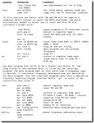
The program "freq" uses TO to count an external pulse train that is known to vary in frequency from io00 to 6000 hertz. T1 generates an exact time delay of 192 microseconds that is counted using registers R4 and R5 of bank I until T1 has overflowed 521d times, or a total delay of. io0032 seconds.
COMMENT
The longer the time taken to count, the more accurate the frequency will be (but remember, it makes litT1e sense to make the readout more accurate than the basic sensor). TO will overflow at 6S,535 or at the end of an interval of io.92 sat fmax, which can be generated in T1 and R4, RS. In this case, the accuracy would be to the nearest .09 hertz (.0001 volt).
If you wish to generate a delay closer to . 1 s than used in the example, make T1 cycle in a shorter period of time and count these shorter periods in R4, RS. Compensate for the 8.5 microseconds it takes for the interrupt routine to determine that time is up.
Preloading TO with a number that causes TO to overflow to 0000 when fmin is present during T will enable TO to read the voltage direcT1y. for our example, presetting TO to FF9Ch will have TO= 01F4h (500d) at fmax = 60,000 hertz for T = .1 s.
Pulse Width Measurement
Theoretically, if the input pulse is known to be a perfect square wave, the pulse frequency can be measured by finding the time the wave is high (Th). The frequency is then
If Th is 200 microseconds, for example, then UF is 2500 hertz. The accuracy of the measurement will fall as the input wave departs from a 50 percent duty cycle.
Timer X may be configured so that the internal clock is counted only when the corresponding I͞N͞T͞X pin is high by setting the GATE X bit in TMOD. The accuracy of the measurement is within approximately one-half of the timer clock period, or .375 microsecond for a 16 megahertz crystal. This accuracy can only be attained if the measurement is started when the input wave is low and stopped when the input next goes low. Pulse widths greater than the capacity of the counter, which is 49.152 milliseconds for a 16 megahertz crystal, can be measured by counting the overflows of the timer flag and adding the final contents in the counter.
For the example in this section, the sensor used to measure the 0 volt to 5 volts de voltage has a fixed frequency of io00 hertz or a period of I ms. For a 0 volt input, the sensor is high for 400 microseconds and low for 600 microseconds; when the sensor input is 5 volts, the output is high for 900 microseconds and low for io0 microseconds. Each volt represents io0 microseconds of time; the accuracy of the measurement is ❗ .00325 volts, which is within the specification of .OJ volt.
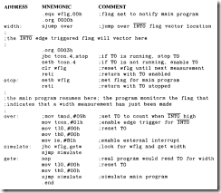
To make the measurement, TO will be configured to count the internal clock when I͞N͞T͞0 is high. The measurement is not started until I͞N͞T͞0 goes from high to low, leaving a minimum of I 00 microseconds to start TO. The measurement is made while I͞N͞T͞0 is high and stopped when I͞N͞T͞0 goes low again. The whole process can be interrupt driven by using the interrupt Hag associated with I͞N͞T͞0 . The IEO flag can be set whenever I͞N͞T͞0 goes from high to low to notify the program to start the pulse width timing and then to stop. A variation of this program is currenT1y in use to measure fabric width by measuring the reflection time of a scanning laser.
Width
The program "Width" measures the width of pulses that are fed to the I͞N͞T͞0 pin, port 3.2 and that are known to vary from 400 to 900 microseconds. The program starts when the interrupt Hag IEO is set and stops the next time the Hag is set, indicating one complete cycle of the input wave.
|
COMMENT |
If there is a considerable amount of electrical noise present on the I͞N͞T͞0 pin, an average value of the pulse width could be found by measuring the widths of a number of consecutive pulses. A counter could be incremented at the end of each cycle and the sum of the widths divided by the counter contents. The noise should average to zero.
Frequency can be measured by timing the interval of a number (M) of high-to-low I͞N͞T͞X interrupts. Synchronize the timing by starting the timer at the first transition. and stop the timer at the Mth + 1 transition. The frequency is then
where T is the count in the timer.
D/ A and A/D Conversions
Conversion between the analog and digital worlds requires the use of integrated circuits that have been designed to interface with computers. Highly intelligent converters are commercially available that all have the following essential characteristics:
Parallel data bus: tri-state, 8-bit
Control bus: enable (chip select), read/write, ready/busy
The choice the designer must make is whether to use the converter as a RAM memory location connected to the memory busses or as an I/O device connected to the ports. Once that choice is made, the set of instructions available to the programmer becomes limited. The memory location assignment is the most restrictive, having only MOVX available. The design could use the additional 32K RAM address space with the addition of circuitry for A 15. By enabling the RAM when A 15 is low, and the converter when A 15 is high, the designer could use the upper 32K RAM address space for the converter, as was done to expand port capacity by memory mapping in Chapter 7. All of the examples examined here are connected to the ports.
D/A Conversions
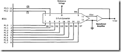
A generic R-2R type D/A converter, based on several commercial models, is connected to ports I and 3 as shown in Figure 8. I 0. Port I furnishes the digital byte to be converted to an analog voltage; port 3 controls the Conversion process. The converter has these features:
Vout = -Yref X (byte in/io0H), Yref = ± io V
Conversion time: 5 µs
Control sequence: ͞C͞S then ͞W͞R
For this example, a io00 hertz sine wave that will be generated can have a programmable frequency. Vref is chosen to be -io volts, and the wave will swing from +9.96 volts to O volt around a midpoint of 4.48 volts. The program uses a lookup table to generate the amplitude of each point of the sine wave; the time interval at which the converter is fed bytes from the table determines the wave frequency.
The Conversion time limits the highest frequency that can be generated using S sample point. In this example, the shortest period that can be used is
FIGURE 8.io DIA Converter Circuit for "Davcon" Program
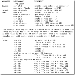
The design tension is high frequency versus high resolution. For a io00 hertz wave, S could be 200d samples. In reality, we cannot use this many samples; the program cannot fetch the data, latch it to port I, and strobe port 3.3 in 5 microseconds. An inspection of the program will show that the time needed for a single wave point is 6 microseconds, and setting up for the next wave takes another 2.25 microseconds. S becomes 166d samples using the 6 microseconds interval. and the addition of 2.25 microseconds at the end of every wave yields a true frequency of io01. 75 hertz.
Davcon
The D/A converter program "Davcon" generates a io00 hertz sine wave using an 8-bit converter. I 66d samples are stored in a lookup table and fed to the converter at a rate of one sample every 6 microseconds. The lookup table is pointed to in external roM by the DPTR, and RI is used to count the samples. Numbers in parentheses indicate the number of cycles.
COMMENT
The program retrieves the data from the highest to the lowest address.
A/D Conversion
The easiest A/D converters to use are the "flash" types, which make Conversions based upon an array of internal comparators. The Conversion is very fast, typically in less than 1 microsecond. Thus, the converter can be told to start, and the digital equivalent of the input analog value will be read one or two instructions later. Modern successive approximation register (SAR) converters do not lag far behind, however, with Conversion times in the 2-4 microsecond range for eight bits.
At this writing, flash converters are more expensive (by a factor of two) than the traditional SAR types, but this cost differential should disappear within four years. Typical features of an eight-bit flash converter are
Data: Vin = Vref (-), data = 00h; Vin = Vref( +),data = FFh
Conversion time: 1 µs
Control sequence: ͞C͞S then ͞W͞R then ͞R͞D
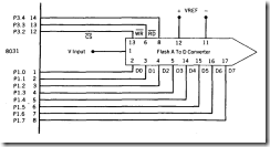
An example circuit, using a generic flash converter, is shown in Figure 8. 11. Port I is used to read the byte value of the input analog voltage, and port 3 controls the Conversion.
FIGURE 8.11 A/D Converter Circuit for "Adconv" Program
A Conversion is started hy pulsing the write line low, and the data is read by bringing the read line low.
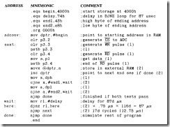
Our example involves the digitizing of an input waveform every l00d microseconds until io00d samples have been stored in external RAM.
Adconv
The program "Adconv " will digitize an input voltage by sampling the input every io0 µs and storing the digitized values in external RAM locations 4000h to 43E7h (l000d samples). Numbers in parentheses are cycles. The actual delay between samples is 99. 75 microseconds.
COMMENT
using this program, we could fill up the RAM in 3.2 s, which illustrates the volumes of data that can be gathered quickly by such a circuit. Realistic applications would feature some data reduction at the microcontroller before the reduced (massaged) data were relayed to a host computer.
Multiple Interrupts
The 8051 is equipped with two external interrupt input pins: I͞N͞T͞0 and INTI (P3.2 and P3.3). These are sufficient for small systems, but the need may arise for more than two interrupt points. There are many schemes available to multiply the number of interrupt points; they all depend upon the following strategies:
Connect the interrupt sources to a common line
Identify the interrupting source using software
Because the external interrupts are active low, the connections from the interrupt source to the I͞N͞T͞X pin must use open-collector or tri-state devices.
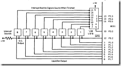
An example of increasing the I͞N͞T͞0 from one to eight points is shown in Figure 8. 12.
Each source goes to active low when an interrupt is desired. A corresponding pin on port I receives the identity of the interrupter. Once the interrupt program has handled the interrupt situation, the interrupter must receive an acknowledgment so that the interrupt line for that source can be Rought back to a high state. Port 3 pins 3.3, 3.4, and 3.5 supply, via a 3-to-8 decoder, the acknowledgment feedback signal to the pRoper interrupt source. The decoder is enabled by port pin 3.0.
Multiple and simultaneous interrupts can be handled by the program in as complex a manner as is desired. If there is no particular urgency attached to any of the interrupts then they can be handled as the port I pins are scanned sequentially for a low.
A simple priority system can be established whereby the most important interrupt sources are examined in the priority order, and the associated interrupt program is run until finished. An elaborate priority system involves ordering the priority of each source. The elaborate system acknowledges an interrupt immediately, thus resetting that source’s interrupt line, and begins executing the particular interrupt program for that source. A new interrupt from a higher priority source forces the current interrupt program to be suspended and the new interrupter to be serviced.
To acknowledge the current interrupt in anticipation of another, it is necessary to also re-arm the I͞N͞T͞X interrupt by issuing a "dummy" RETI instruction. The mechanism for accomplishing this task is illustrated in the program named "hipri." First, a low priority scheme is considered.
FIGURE 8.12 Multiple-Source Interrupt Circuit Used in "Lepri" and "Hipri" pograms
Lopri
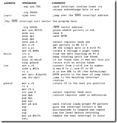
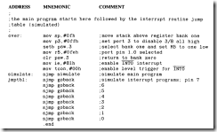
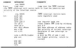
The program "Lopri " scans port Pl for the source of an interrupt that has triggered I͞N͞T͞0 . The pins are scanned for a low and the scan resumed after any interrupt is found and serviced. The interrupt source is acknowledged prior to a RETI instruction. R5 of bank I is used to store the next pin to be scanned, and R6 is used to scan the pins for a low. A jump table is used to select the interrupt routine that matches the particular interrupt. Each interrupt routine supplies the 3-to-8 decoder a unique acknowledge pattern before a RET1.
The instruction JMP @A+DPTR has been used to select one of a number of jump addresses, depending upon the number found in A. The simulated subroutines could be an SJMP to the actual interrupt handling subroutine. Because each SJMP takes two bytes to execute, A has to be doubled to point to every other byte in the jump table. When this action is not convenient, A can use a lookup table to get a new A, which then accesses a jump address.
RS has one bit low, and that bit acts as a mask when ORed with P1 to find the low bit in P1 When the low pin does not match the RS pattern, the RETI will immediately cause I͞N͞T͞0 to interrupt again, and RS will be set to the next pin position. The worst-case response time, if eight pins must be searched before the low pin is found, will be in the order of 600 microseconds.
If I͞N͞T͞0 is triggered by noise, the routine returns after the first fruiT1ess search with no action taken and re-arms the interrupt structure.
The external interrupt flags are cleared when the program vectors to the interrupt address only when the external interrupt is edge triggered. Level triggered interrupts must have the low level removed before the RETI, or an immediate interrupt is regenerated. Each interrupt routine loads the internal RAM location "ack" with the proper bit pattern to the decoder to enable and decode the proper line to reset the interrupting source.
Hipri
Suppose that we wish to have a priority system by which the priority of each input pin is assigned at a different level-that is, there are eight priority levels, and each higher level can interrupt one at a lower level. Theoretically, this leads to at least nine return addresses being pushed on the stack (plus any other registers saved), so the stack should be expected to grow more than 18d bytes; it is set above the addressable bits at location 2Fh.
In order to enable the interrupt structure in anticipation of a higher level interrupt, it is necessary to issue a RETI instruction without actually leaving the interrupt routine that
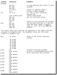
currently has the highest priority. One way to accomplish this task is to push on the stack the address of the current interrupt routine to be done. Then, use a RETI that will return to the address on the stack, the desired current interrupt subroutine, and also re-arm the interrupt structure should another interrupt occur. The addresses of each subroutine can be known before assembly by originating each at a known address, or the program can find each address in a lookup table and push it on the stack, as illustrated in the example program.
For this example, the priority of each interrupt source is equivalent to the port I pin to which its identity line is connected. Pl .0 has the highest priority, and Pl .7, the lowest. A lookup table is used to find the address of the subroutine to be pushed on the stack.
External interrupt I͞N͞T͞0 is connected to the common interrupt line from all sources. It is enabled edge triggered whenever an interrupt routine is running so that any higher priority interrupt will be immediately acknowledged. If a lower priority interrupt occurs, it will interrupt the program in progress long enough to determine the priority. The interrupted subroutine will resume, and the lower level interrupt source priority will be saved until the subroutine in progress is finished. All interrupting sources maintain their identity lines low until they are acknowledged. The common interrupt line is reset immediately to enable any other source to interrupt the 8051.
If a higher level source interrupts a lower priority interrupt, then the high priority routine will interrupt the lower priority routine. The priority of the lower level interrupt will he saved.
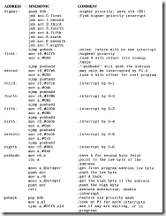
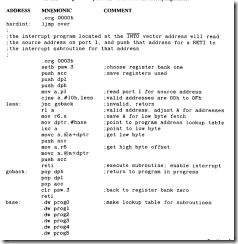
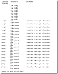
The program "Hipri" assigns eight levels of priority to the interrupt sources connected to port I . A lookup table is used to find the address of the interrupt handling subroutine that is pushed on the stack. A RETI instruction is then used to "return" to the desired subroutine and re-arm the interrupt hardware on the 8051.
COMMENT
The .dw assembler directive will store the high byte of the two-byte word at the lower address in memory. For the RETI in "pushadd" to work properly, the low address byte must be placed on the stack first.
If interrupt A has just gone low, and interrupt B, which is of a higher priority, occurs after the system has vectored to the I͞N͞T͞0 address, interrupt B will be accessed if the B line goes low before the polling software starts (INB ACC.x). If the polling has caused A to be chosen, then B will be recognized alter the RETI in "pushadd" causes the A address to be POPed from the stack. One instruction of A will be executed, then the IEO flag in TCON will cause an interrupt.
The 8051 interrupt system will generate an interrupt unless any of the following conditions are true:
Another routine of equal or greater priority is running. The current instruction is not finished.
The instruction is a RETI or any IE/IP access.
The edge-triggered interrupt sets the IEO flag, and the interrupt that generated the edge serviced after any of the listed conditions are cleared.
Hardware Circuits for Multiple Interrupts
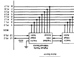
Solutions to the expanded interrupt problem proposed to this point have emphasized using a minimal amount of external circuitry to handle multiple, overlapping interrupts. A hardware strategy, which can be expanded to cover up to 256 interrupt sources, is shown in Figure 8.13. This circuit is a version of the "daisy chain" approach, which has long been popular.
The overall philosophy of the design is as follows:
1. The most important interrupt source is physically connected first in the chain, with those of lesser importance next in line. Lower priority interrupt sources are "behind" (connected further from I͞N͞T͞0 ) those of a higher priority.
2. Each interrupting source can disable all signals from sources that are wired behind it. All sources that lose the INACTOUT signal (a low level) from the source(s) ahead of it will place their source address buffer in a tri-state mode until INACTOUT is restored.
3. A requesting source pulls its I͞N͞T͞0 UT line low and places its 8-bit identifier on the tri-state bus connected to port I . The interrupt routine at the I͞N͞T͞0 vector location reads Pl and, using a lookup table, finds the address of the subroutine that handles that interrupt. The address is placed on the stack and a RETI executed to go to that routine and re-arm the interrupt structure.
4. The interrupt subroutine generates an ACKIN signal (a low-level pulse) to the source from the 805 I at the end of the subroutine; the source then removes I͞N͞T͞0 UT and the 8-bit source address. When an interrupt is acknowledged, the interrupting source must bring the I͞N͞T͞0 UT line high for at least one machine cycle so that the 8051 interrupt structure can recognize the next high-to-low transition on I͞N͞T͞0 .
The software is very simple for this scheme. Any interrupt received is always of higher priority than the one now running, and the source address on port I enables rapid access to the interrupt subroutine.
Accomplishing this interrupt sequence requires that the source circuitry be complex or that the source contain some intelligence such as might be provided by a microcontroller.
The additional source hardware will entail considerable relative expense for each source. As the number of interrupt sources increases, system costs rise rapidly. At some point the designer should consider another microcontroller that has extensive interrupt capability.
Hardint
The program "Hardin!" is used with daisy-chained interrupt sources to service 16 interrupt sources. An interrupt is falling-edge triggered on I͞N͞T͞0 and the interrupt address read on PI. A lookup table then finds the address of the interrupt routine that is pushed on the stack and the RETI "returns" to the interrupt subroutine. The interrupt subroutine issues an acknowledgment on port 3.3, which resets the interrupting source.
COMMENT
lf the lookup table goes beyond 128 addresses, or 256 bytes, then DPH is ncremented by one to point to a second complete table.
Each interrupt subroutine must contain an acknowledge byte that is placed on P3 to reset each source.
Note the use of CINE and the carry flag to determine relative sizes of two bytes at label "less."


