ILLUSTRATIVE EXAMPLE 3: APPLIANCE CONTROL USING MEMORY-MAPPED I/O TECHNIQUE
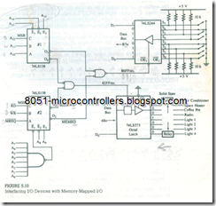
Figure 5.10 shows a schematic of interfacing I/O devices using the memory mapped I/O technique. The circuit includes one input port with eight DIP switches and one output port to control the appliances. The appliances are turned on and off by the microprocessor according to the corresponding switch positions. For example, the switch S7 controls the air conditioner and the switch S0 controls Light 4. All switch inputs are tied high; therefore, when a switch is open (off), it has + 5 V, and when a switch is closed (on), it has logic 0. The circuit includes two 3-to-8 decoders and one 8-input NAND gate to decode the address bus and generate the control signals. The eight switches are interfaced using a tri-state buffer 74LS244, and the appliances are interfaced using an octal latch (74LS373) with tri-state output.
5.6.1 Control Signals
In a memory-mapped I/O circuit, the control signals required are M̅R̅E̅Q̅ (Memory Request) and Read (R̅D̅) or Write (W̅R̅).In this circuit (Figure 5.10), they are used as inputs to a 3-to-8 decoder (labelled #2) to generate additional control signals. The enable lines of the decoder are controlled by the address lines. Assuming the
decoder is enabled by the appropriate address, we need to analyze the input and identify the output lines of the decoder that can be used as control signals.
To assert the Memory Write (M̅E̅M̅W̅R̅) signal, the input should be M̅R̅E̅Q̅= 0, W̅R̅= 0, and R̅D̅= 1 (R̅D̅ and WR cannot be active at the same time). With this input, the output line O4. goes active and generates the MEMWR signal.
To assert the Memory Read (M̅E̅M̅R̅D̅) signal, the input should be M̅R̅E̅Q̅= 0, W̅R̅ = 1, and R̅D̅ = 0. With this input to the decoder, the output O2 goes active and generates the M̅E̅M̅R̅D̅ signal.
5.6.2 Output Port and Its Address
The appliances are connected to the data bus through the latch 74LS373 and solid state relays. If an output bit of the 74LS373 is high, it activates the corresponding relay and turns on the appliance, which remains on as long as the bit stays high. Therefore, to control the appliances, we need to supply the appropriate bit pattern to the latch.
Figure 5.10 shows that the O̅E̅ of the latch is connected to the ground; thus, the latched data will keep the relays on or off according to the bit pattern. The LE is connected to the I/O select pulse, which is asserted when the output 00 of decoder #1 and the control signal M̅E̅M̅W̅R̅ go low. Therefore, to assert the I/O select pulse, the output port address should be 82FFH•
5.6.3 Input Port and Its Address
The DIP switches are interfaced with the Z80 using the tri-state buffer 74LS244. The switches are tied high and are turned on by grounding shown in Figure 5.10. The switch positions can be read by enabling the signal O̅E̅ (O̅E̅1 and O̅E̅2), which is asserted when both the output O1 Of decoder #1 and the control signal M̅E̅M̅R̅D̅ go low. Therefore, to read the input port, the port address should be 86FFH•
5.6.4 Instructions
To control the appliances according to switch positions, the microprocessor should read the bit pattern at the input port and send that bit pattern to the output port. The following instructions can accomplish this task.
When this program is executed, the first instruction reads the bit pattern 1 0 1 1 0 111 (B7H) at the input port 86FFH and places that reading in the accumulator; this bit pattern represents the “on” position of switches S6 and S3 The second instruction complements the reading; this instruction is necessary because the “on” position has logic 0, and logic 1 is necessary to turn on solid state relays. The third instruction sends the complemented accumulator contents (0 I 00 I 000 = 48H) to the output port 82FFH. The 74LS373 latches the data byte 0 1 0 0 1 0 0 0 and turns on the space heater and Light 1. The last instruction, JP READ, takes the program back to the beginning and repeats the loop continuously in order to monitor the switches.


