Memory Map
Typically, in an 8-bit microprocessor system, 16 address lines are available for memory. This means it is a numbering system of 16 binary bits and is capable of identifying 216 (65,536) memory registers. each register with a 16-bit address. The entire memory addresses can range from 0000 to FFFF in Hex. A memory map is like a pictorial representation in which memory devices are located in the entire range of addresses. Memory addresses provide the locations of various memory devices in the system, and the interfacing logic defines the range of memory addresses for each memory device.
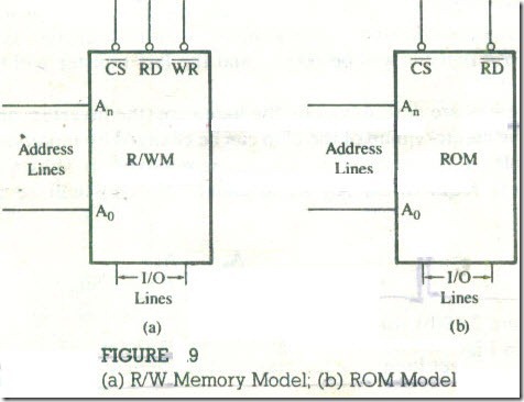
Figure 9
(a) RIW Memory Model; (b) ROM Model
Now let us assume that we have a memory chip with 256 registers that needs only eight address lines (28 = 256). How can we assign 16-bit addresses to 256 registers? This can be accomplished by using the remaining eight lines for the Chip Select through appropriate logic gates as illustrated in the next example.
Example 1
Illustrate the address range of the memory chip with 256 bytes of memory, shown in Figure 10(a), and explain how the address range can be changed by modifying the hardware of the Chip Select CS line in Figure 10(b) .
solution
Figure 10(a) shows a memory chip with 256 registers with 8 I/O lines; the memory size of the chip is Chip Select CS’ signal (active low), and two control signals Read (RD) and write (WR). The eight address line (A7-A0) of the microprocessor are required to identify 256 memory registers. The remaining eight lines (A15-A8) are connected to the chip Select (CS) line through inverters and the NAND gate .The memory chip is enabled or selected when CS goes low. Therefore, to select the chip ,the address lines A15-A8 should be at logic 0,which will cause the output of the NAND gate. to go low .No other logic levels on the lines A Is-AM can select the chip. Once the chip is selected (enabled). the remaining address lines A/An can assume any combination from 00H to 00FFH and identify any of the 256 memory registers through .its decoder Therefore, the memory addresses of the chip in Figure 10(a) will range from 0000H to 00FFH as shown below.
Chip Enable or Chip Select Register Select
The address of the first memory register is 0000H, and the address of the last register is 00FFH. If we numbered these registers in decimal with a four-digit system, the address of the first register will be 000010, and the last register will be 025510.
The chip select addresses are determined by the hardware (the inverters and ‘NAND gate); therefore, the memory map of the chip can be changed by modifying the hardware. For example, if the inverter on line Allis removed as shown in Figure 10(b). the address required on A15-A8 to enable the chip will be follows:
The memory map for Figure 10(b) will be 8000H to 80FFH·
The memory chips in Figures I0(a) and (b) are the same chips. However by changing the hardware of the Chip Select logic, the location of the memory in the map can be changed ,and memory can be assigned addresses in various locations over the entire range of 0000 to EFFF .
Example 2
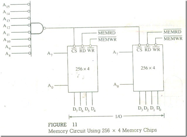
In Figure 10(a), how many 256 x 4 memory chips would be required to replace the 256 x 8 memory chip’? Redraw Figure 10(a) using 256 x 4 memory chips.
solution
The memory chip with the size of256 x 4 has 256 registers, and each register has four data or 110 lines. Therefore, we would need two 256 x 4 memory chips to replace the 256x 8 memory chip as shown in Figure 11. The address lines A1 to A0 and CS’ line will be the same for both chips; however. data lines D7 to D4 will be connected to the first chip, and the lines D3 to D0 will be connected to the second chip.
In a memory system, a l6-bit address can be conceptually organized into two groups of Hex number .With two Hex digits, 256 registers can be numbered from 00H to FFH as shown in Example 1. This is defined as a page with 256 lines (registers) 10 read from or write on. Similarly ,high-order Hex digits in an address can be used to number the pages from 00H to FFH ; thus, the total range of 64K can be conceptually divided into 256’pages with each page having 256 lines. For example. the memory address 020FH represents line (register) 15 on page 2. and the address 07FFH represents register 255 on page 7. A memory chip with IK (1,024) byte can be viewed as a chip with four pages. This is just a convenient way of thinking about memory addresses.
Another way of viewing a memory address is in terms of high-order and low order addresses. The lines used for chip select are called high-order address lines, and the lines connected to memory address lines are called low-order address lines. Let us use an example of a four-digit (decimal) numbering system in a highrise apartment building. Generally, the first two digits (high-order) represent a floor and the last two digits (low-order) represent an apartment number. To locate apartment 1241. we go first to the twelfth floor (similar to Chip Select in memory addressing), and then we look for the apartment 41 (similar to selecting a register). Now let us use the example of an apartment complex. Let us assume the complex is divided into sections I to 9, and each section has up to 999 apartments. In this situation, the number 245) would represent Section 2 and apartment number 451; the digit 2 is a high-order address. and 451 is a low-order address. This is similar to memory addresses of 1 K memory. The I K memory chip will require 10 address lines. and the remaining six lines of the address bus will be used for the CS’. Thus, the group of six address lines will be high order, and the remaining ten address lines will be low order. The memory addresses will be determined by combining the logic levels of these address lines. If the number of address lines in a microprocessor is larger than 16, we will use a five-digit Hex numbering scheme.
Example 3
If the address range of a memory chip is from 4000H to 43FFH, calculate the number of memory registers in the chip.
Solution
The number of registers in Hex: 43FFH – 4000H = 3FFH
The decimal equivalent of 3FFH = 1023
Therefore, the total number of registers in the chip = 1024 (I K). To include the first address, we need to add one to the calculated value.
How the MPU Writes into and Reads from Memory
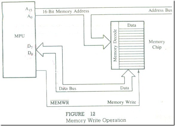
To store (write) a byte into a memory location (Figure 12), the MPU
1. Places the 16-bit address on the address bus of the memory location where a byte is to be stored .The interfacing logic of the memory chip decodes the address and selects the memory register-to be written into.
2. Places the byte on the data bus.
3 . Send the control signal Memory Write to enable the input buffers of the memory and then stores the byte.
To read from memory the steps are similar to that of writing into memory, except the order of steps 2 and 3.
1. The MP places the 16-bit address on the address bus of the memory location from where a byte is to be read. The interfacing logic of the memory chip decodes the address and selects the appropriate memory register.
2. The MPU sends the control signal Memory Read to enable the output buffer of the memory chip.
3. The memory chip places the data byte on the data bus ,and the MPU reads the data byte.
FIGURE 12
Memory Write Operation


