MEMORY
Memory is an essential component of a microcomputer system; it stores binary instructions and data for the microprocessor. There are various types of memory, and they can be classified in two groups: prime (or main) memory and storage memory. In the last chapter. we saw two examples of prime memory: Read/Write Memory (R/WM) and Read-Only Memory (ROM). Magnetic tapes and disks can be cited as examples of storage memory. First. we will focus on prime memory and then briefly discuss storage memory when we examine various types of memory.
The R/W memory is made up of registers, and each register has a group of
flip-flops or field-effect transistors that store bits of information. The user can use this memory to hold programs and store data. On the other hand, the ROM stores information permanently in the form of diode ; the group of diodes can be viewed as a register. In a memory chip. all registers are arranged in a sequence and identified by binary numbers called memory addresses. The MPU uses its address bus to send the address of a memory register and uses data and control buses to read from or write into that register. In the following sections, we examine the basic concepts related to memory-its structure, its addresses. and its requirements for communication with the MPU-and build a model for RJW memory. However, the discussion is equally applicable to ROM except for slight differences in Read! Write control signals.
Flip-Flop or Latch as a Storage Element
What is memory? It is a circuit that can store bits-generally high or low voltage levels representing 1 and O. A flip-flop or a latch is a basic element of memory.
FIGURE 4
Latches as Storage Elements
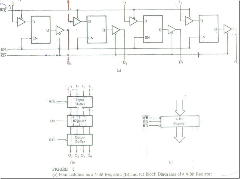
To write or store a bit in the latch. we need an input data bit and an enable signal (Figure 4(a)) . In this latch, the stored bit is always available on the output line. If a tri-state buffer is connected to the output of the latch(as shown in Figure 4(b) , the stored bit can be read only when the buffer is enabled . Similarly. we can also use a tri-state buffer on the input of the latch. Now we can write into the latch (Figure 4(c)) by enabling the input buffer and read from it by enabling the output buffer. This latch. which can store one binary bit. is called a memory cell. Figure 5(a) shows four such cells or latches grouped together to form a register that has four input lines and four output lines and can store four bits. The size of this register is specified as either 4-bit or 1 x 4 bit which indicates one register with four cells or four I/O lines. The number of bits stored in a register is called a memory word. Figures 5(b) and (c) show simplified block diagrams of the 4- bit register.
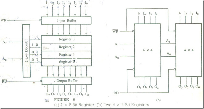
In Figure 6(a), four registers with eight cells (or 8-bit memory word) are arranged in a sequence :to write into or read from anyone of the registers. specific register should be identified or enabled .This is a simple decoding function :a 2-to-4 decoder can perform that function. However. two more input lines A1 and A0, called address lines. are required to the decoder. These two input lines can carry four different bit combinations (00. 01. 10, 11), and each combination can identify or enable one of the registers named as Register 0 through Register 3.
In Figure 6(a), the chip has an 8-bit memory word, and its size can be specified as 32 bits, 4 x 8 bits, or 4 bytes. If we have a memory chip with a 4-bit memory word, we can combine two such chips in parallel to make an 8-bit memory word as shown in Figure 6(b). The address lines and RD/WR control signals ( -indicates active low) will be connected in parallel, but the memory word will consist of 4 bits from each chip as shown.
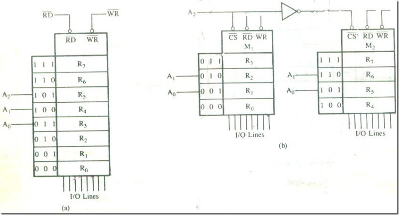
Now we can expand the number of registers. If we have eight registers on one chip, we need three address tines and a 3-to-8 decoder. an interesting problem is how to deal with two chips with four registers each . We have a total of eight registers ; therefore, we need throe address lines. One address line. A,. is used to select a chip, and the address lines A1 and A0 are connected to both chips.
FIGURE 6
(a) 4 x 8 Bit Register; (b) Two 4 x 4 Bit Registers
Figure 7(b) shows that the Chip Select signal CS’ is active low .so that when A2 is 0 (low). Chip M1 is selected and when A2 is 1 (high), Chip M2 is selected. The addresses on A1 and An will determine the registers to be selected; thus. by combining the logic on A2. A1. and A0. the memory addresses range from 000 to 111. The concept of the Chip Select signal gives us more flexibility in designing chips and allows us to expand memory size by using multiple chips.
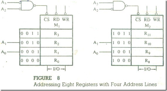
Now let us examine the problem from a different perspective. Assume that we have available four address lines and two memory chips with four registers each as before .Four address lines are capable of identifying sixteen (24) registers: however ,we need only three address lines to identify eight registers .What should we do with the fourth line? One of the solutions is shown in Figure 8. Memory chip M1 is selected when A3 and A2 are both 0; therefore. registers in this chip are identified with the addresses ranging from 0000 to 0011 (0 to 3). Similarly. the addresses of memory chip Ml range from 1000 to 1011 (8 to B); this chip is selected only when A3 is 1 and A2 is 0. In this example. we need three lines to identify eight registers. two for registers and one for Chip Select. However. we used also the fourth line for Chip Select. This is called complete or absolute decoding. Another option is to leave the fourth line as "don’t care"; we will further explore this concept later.
After reviewing the above explanation, we can summarize the requirements of a memory chip as follows:
FIGURE 7
(a) Memory Chip with Eight Registers; (b) Two Memory Chips with Four Registers Each
1. A memory chip requires address lines to identify a memory register, a Chip. Select CS’ signal to enable the chip, and control signals to read from and write into memory registers.
2. The number of address lines required is determined by the number of registers in a chip (2n = Number of registers where n is the number of address lines).
3. If additional address lines are available in a system. they are used to enable the Chip Select CS’ signal. The memory address of a register is determined by
FIGURE 8
Addressing Eight Registers with Four Address Lines
the logic levels (011) of all the address lines (including the address lines used for CS’).
4. The control signal Read (RD’) enables the output buffer. and data from the selected register are made available on the output lines. Similarly, the control signal Write (WR’) enables the input buffer, and data on the input lines are written into memory cells.
A model of a typical memory chip representing the requirements just stated is shown in Figure 9. Figure 9(a) represents the R/W memory and Figure 9(b) represents the Read-Only Memory; the only difference between the two as far as addressing is concerned is that ROM does not need a WR’ signal. Internally, the memory cells are arranged in a matrix format (in rows and columns), because as the size increases the internal decoding scheme we discussed becomes impractical. For example, a memory chip with 1024 registers would require a 10-to-1024 decoder. 1f the cells are arranged in six rows and four columns, however. the internal decoding circuitry can be designed with two decoders, one for-selecting a row and the other for selecting a column. The internal row and column arrangement does not affect our external interfacing logic.


