FPGA-Based Switching Controller
A phase-shift or level-shift can be introduced between the carrier signals of contiguous cells to produce a phase-shifted or level-shifted switching pattern between them. In this way, when connected together a staircase multilevel waveform is synthesized. For m-level converter, (m-1) phase-shifted or line-shifted carriers are needed. The phase-shifted carriers are specially conceived for FC [23] and MMC [24] converters and level-shifted carriers are especially useful for NPC converter. Figure 9 shows the basic block diagram of switching controller.
One compare unit is used for each half-bridge of the H-bridge inverter cell or each pair of active switching devices; the compare units compare the carrier signal with a reference signal. Each compare unit generates one switching signal for the top switching device. The inverted form of this switching signal drives the bottom switching device. The four carrier signals and the three reference signals as required by the 3-phase 5-level multilevel converter are shown in Fig. 10.
The performance of DSP is limited by the clock rate, and the number of useful operations per clock. In addition, the available DSP at present only can provide
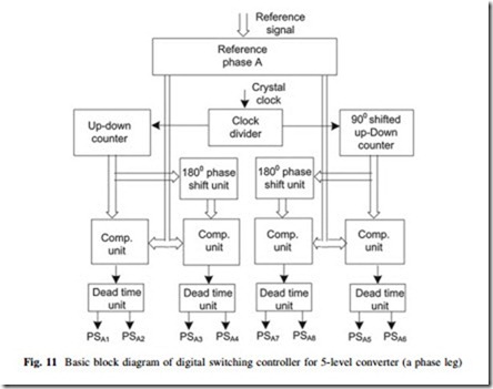
about six pairs of PWM channels, which is clearly insufficient for multilevel inverter systems (e.g., a 3-phase 5-level modular multilevel inverter requires 24 PWM signals). In this chapter, a fully digital switching control scheme is developed and implemented with an Xilinx XC3S500E FPGA. The most common software such as the MATLAB/Simulink and Xilinx ISE-based design technique is used to develop the switching controller, which may save the development time and cost of the switching controller. Figure 11 shows the basic block of the digital switching controller. In this technique, the switching control scheme with target system is modeled in the MATLAB/Simulink environment first.
After having achieved satisfactory performance from the Simulink, the updated model is used for behavioral modeling of the switching controller in the Xilinx ISE environment. The behavioral simulation results were observed, and they were found highly consistent with the Simulink results. After having acquired satisfactory simulation results, the design was implemented and verified with timing simulation. Before connecting with the target system, the gate signals were measured and they were found highly consistent with the Simulink results and the theoretical values.
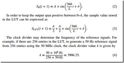
In total, three reference signals are required, one for each phase leg. A look-up table (LUT) is used to generate the reference signals, which makes the control circuit totally digital and integrated. Including the inverted carrier signals, a total of four carriers are able to generate four gate pulses when comparing them with a reference signal. The other four gate pulses can be generated by just inverting these four gate pulses with a consideration of the deadtime. In this project, 9-bit up-down counters are used to generate phase-shifted carrier signals. An LUT is actually a set of memory locations which contains the sampled values of a desired analog signal. The frequency of the sine wave can be increased by skipping entries in the sine LUT as the angular resolution depends on the number of entries, for a cycle. If A is the amplitude of the reference signal, d the phase angle, L the number of entries, and i varies from 0 to (L-1), the sample value can be calculated as
The sample values of the reference signals can be calculated from Eq. (3). The reference signals for phases A, B, and C can be generated by considering the values of d as 0°, 120°, and -120°, respectively. A very high speed integrated hardware description language (VHDL) code-based program is used to create the LUT, which contains the sine reference.

