This chapter discusses the criteria for evaluating the next generation wind power converter. The importance of thermal stress in the power semiconductors is emphasized by relating it with the reliability and cost performances. Then a multidisciplinary approach for the stress analysis of wind turbine system is introduced, where the factors of converter design, converter control, wind speed, and grid codes are all taken into account.
Importance of Thermal Stress in Wind Power Converter
In the past, the power electronics are not so important in the wind power application and they just need to carry little or partial power produced by the wind turbines. As a result when designing the converter system, the losses generated by the power electronic components are not so significant and the voltage/current ratings were mainly focused.
However, the power electronics nowadays are used to handle full generated power from the wind turbines even up to 8 MW; the loading and loss of power electronic components become much more severe. Considering the limited space in the nacelle or tower of wind power application, it is more and more difficult to achieve satisfactory cooling environment for the internal parts, resulting in adverse thermal stress of the power electronic devices. Consequently, not only the power handling ability but also the loss/thermal behaviors have to be carefully taken into account when designing the next generation wind power converter.
As one of the most important loading indicators, the thermal stress is found to be closely related to the reliability, cost, and power density of the converter system, as will be illustrated in the following.
Thermal Stress Versus Reliability
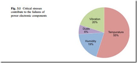
According to the statistics carried by [1], the proportion of various stresses that contribute to the failures of power electronic components is shown in Fig. 3.1. It can be seen that there are 55 % of the component failures which are caused by the temperature or thermal stresses. It is noted that the stress distribution in Fig. 3.1 could be varied depending on the application; however, as reported in [2–5] it is generally accepted that the thermal loading is an important “trouble maker” for most of the failure mechanisms in the electronic devices, like capacitor, printed circuit board, power semiconductors, etc.
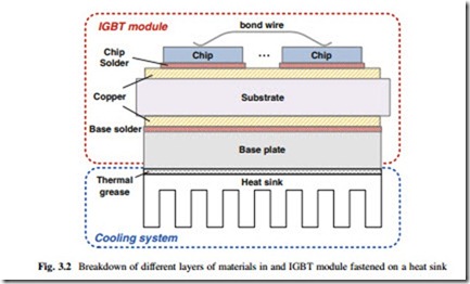
Figure 3.2 shows a breakdown of different layers inside a IGBT module [6], which is chosen here as an example because it has been a popular power semi- conductor technology used in almost all power converter applications. It was found that the main driver for the IGBT failures is the thermal cycling of different layers of materials with mismatching expansion coefficients: The losses generated from the silicon chips periodically propagate through a couple of materials to the heat sink, causing temperature excursions on different layers, which then expand and compress until cracks or disconnections are triggered. It has been widely recognized that the three dominant failure mechanisms for IGBT modules are the bond wire lift-off, solder joints cracking under the chip, and solder joints cracking under the substrate, as also indicated in Fig. 3.2 [7–9]. As for the press-pack IGCT or IGBT, although the quantified failure models are not established yet, it is found that the thermal stress is also an important cause of problems for these devices [6].
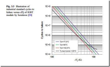
Nevertheless, it has been proved that the thermal stress and lifetime of IGBT modules can be mathematically correlated, as summarized in [6, 8], where a series of lifetime models are introduced. Normally the parameters of these lifetime models need to be acquired experimentally by accelerating tests, in which the power devices are running at various thermal loadings and the failures are observed and recorded. Afterwards, some mathematical functions are used to fit these recoding points e.g., Coffin-Masson model [8]. Figure 3.3 shows an example of the lifetime
testing results provided by Semikron, in which several fitting curves are plotted to represent the relationship between the cycles to failure of a series of IGBT modules and the applied thermal stresses—in this case the junction temperature excursion ΔTj and the mean junction temperature Tjm.
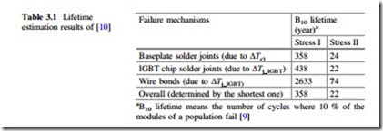
In [10], the similar model as Fig. 3.3 is utilized in a wind power converter to estimate the lifetime of the power devices subjected to a series of wind profiles. The estimated results are listed in Table 3.1, where two thermal stress levels are applied
and the lifetime in respect to the three failure mechanisms of IGBT module are indicated respectively. It is obvious that the thermal stress has significant impacts to the reliability of the power semiconductor devices and their relationship can be analytically correlated.
Thermal Stress Versus Cost
The thermal stress of power semiconductors is determined by many design factors like the rating margins, packaging technology, heat sink design, circuit topologies, etc., which are all related to the cost of the converter. A straight forward example is that if the power devices are used to convert the same amount of power with larger power ratings and using a more powerful heat sink, the junction temperature will be more or less relieved with drawback of the increased cost.
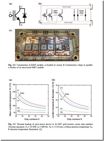
Therefore, it should be possible to correlate the thermal stress and the cost of converter. As shown in Fig. 3.4, where the symbol in circuit, real construction, and uncovered picture of a IGBT module are illustrated, it is noted that actually the IGBT module is composed of many IGBT/Diode silicon chips in parallel internally, and the number of the paralleled chips will determine the current rating and thereby the size of IGBT module; therefore, the chip numbers can be an easier quantified parameter for the cost of the converter.
In the special topic attached Chap. 9, a thermal-cost model which correlates the junction temperature of IGBT module and the corresponding parallel silicon chip numbers is established.
In the attached special topic Chap. 9, the thermal-cost model is demonstrated on a 10-MW 3L-NPC wind power converter. One of the analyzing results is shown in Fig. 3.5: the vertical axis represents the junction temperature in different power devices of the 3L-NPC converter, and the horizontal axis represents the corresponding paralleled chip numbers in the IGBT module. The mean junction tem- perature Tm and the temperature fluctuation ΔTj are both shown, respectively, in Fig. 3.5 a, b. It can be seen that the thermal stress also has significant impacts to the rating/cost of the power semiconductor devices and their relationship can be analytically correlated.
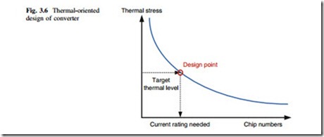
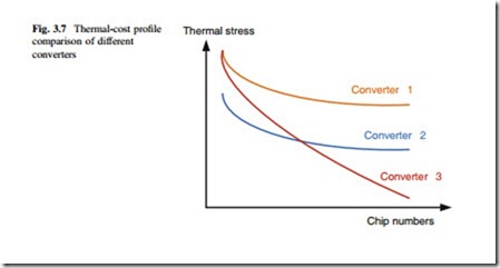
With the established thermal-cost relationship, more advanced design and evaluation of wind power converter can be realized, as demonstrated in the attached topic (Chap. 9). For example, it is possible to select the “just right” current rating of the power device to achieve the target junction temperature, as shown in Fig. 3.6. Thereby more cost-effective converter design can be achieved especially for the multi-level converters with unequal loading of the power devices. Also it is possible to unify various converters under the same thermal-cost domain, as shown in Fig. 3.7, enabling a more sensible comparison of different converter solutions.
According to the illustrations of thermal-related models as well as their utilization in the wind power converter, it can be revealed that the thermal stress is closely related to the reliability and cost of the power electronic components. Moreover, as shown in Figs. 1.9, 1.10 and 1.11, many grid codes have regulations for the delivered reactive/active power by wind turbines and thereby will also change the operating condition of converter in respect to the current, voltage,
phase-angle, and the loading of power devices. As a result, the thermal stress is an important performance to be deeply investigated for the next generation wind power converter.
