Regardless of the type of trouble symptom, the actual fault can be traced eventually to one or more of the circuit components (vacuum tubes, transistors, ICs, diodes, resistors, capacitors, coils, transformers, and so forth). The checks of wave forms, voltage, and resistance will then indicate which branch within a circuit is at fault. Finally, you must locate the particular component that is causing the trouble in the branch.
In order to do this, you must be able to read a schematic diagram. These diagrams show what is inside the blocks on a servicing block diagram and provide the final picture of the electronic equipment. Often, you must service equipment with the aid of nothing more than a schematic diagram. If you are fortunate, the diagram will show some voltages and wave forms.
Figure 1 2 shows the schematic diagram of a solid state radio receiver. This receiver unit (a portable broadcast radio) differs considerably from the one illustrated in the servicing block diagram shown in Fig. 1 19. For example, in the receiver shown in Fig. 1 2, there is no RF amplifier; the frequency converter (mixer and RF oscillator) function is accomplished by one transistor, Qx ; there are only two IF amplifiers (one not shown); and there is no phase splitter in the audio section.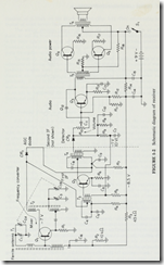
Examples of using schematic diagrams.
The following examples demonstrate the use of the schematic diagram to locate a fault within a circuit. Although these examples involve a simple portable transistor radio, the same basic troubleshooting principles apply to more complex equipment.
In order to follow these examples properly, you must be able to use basic test equipment. If you are unsure of how such test equipment is used in troubleshooting, read Chapter 2 before you study these examples. (You may also read Chapter 2 in conjunction with these examples.)
Example 1. Assume that the receiver shown in Fig. 1 2 is being serviced and that the trouble is isolated to the frequency converter. This is done by injecting a signal of appropriate frequency (IF) modulated by an audio tone at the IF input (the primary winding of transformer T3 ). A good response is heard on the loudspeaker. However, no response is obtained when a signal of proper frequency (RF) is injected at the primary winding of Tx with the receiver tuned to that frequency.
The next step is to measure the voltages at the collector, emitter, and base of Qx (in that order), as shown in Fig. 1 42. If any of the Q x elements show an abnormal voltage, the resistance of the element should be checked first. Note that the collector voltage is specified as —7 V. Neither the base and emitter voltages nor any of the resistance values are given. This lack of information is typical of electronic equipment used for home entertainment. Thus, you must be able to interpret schematic diagrams to estimate approximate voltages.
For example, the voltage at the junction of R3 and RA is given as —8.5 V. This is logical because the source (a battery) is 9 V. The value of R2 is approximately 25 percent of the value of R3 . Thus, the drop across R2 is about 25 percent of —8.5 V, or approximately —2 V, and the base of Ql should be about —2 V. If Qx is silicon, the emitter will be about 0.5 V different from the base, or about —1.5V (emitter more positive or less negative, in this case). If Qx is germanium, the base emitter differential will be about 0.2 V, and the emitter should be approximately —1.8 V.
Keep in mind that this method of interpreting the schematic will give you approximate voltages only. In practical troubleshooting, the voltage differentials between circuit elements and transistor electrodes are the most important factor. Troubleshooting solid state equipment based on voltage differentials is discussed fully in Chapter 3.
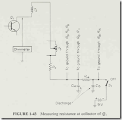
Now, assume that there is no voltage at the collector but that the base and the emitter show what appear to be normal or logical voltages. The next step is to remove power, discharge C, 4 and C15 (if necessary), and measure the collector resistance (to ground), as shown in Fig. 1 43. Because no resistance values are given, you must use the schematic to estimate the approximate values.
Of course, if you find a zero resistance at the collector, this indicates a short. For example, capacitor C5 could be shorted. On the other hand, an infinite resistance indicates an open circuit. For example, the coil windings of T 2 and T 3 could be open, or R 4 could be burned out and open. It is usually easy to locate the fault when you find such extreme resistance readings.
However, a resistance reading that falls between these two extremes does not provide a really sound basis for locating trouble. To make the problem worse, the effect of solid state devices in the circuit can further confuse the situation.
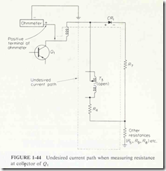
For example, assume that the fault is an open T 3 winding, as shown in Fig. 1 44. This will result in a no voltage reading at the collector of Q 1 • However, it is still possible to measure a resistance to ground from the Q 1 collector if the following conditions are met: Assume that the ohmmeter leads are connected so that the positire terminal of the ohmmeter battery is connected to the Q 1 collector. This will forward bias the automatic gain control (AGC) diode CR 1 and cause the ohmmeter to measure the resistance across R7 (the collector supply of Q2 ). Also. if the collector of Q , is made positive in relation to the base, the Qx base collector junction will be forwardbiased, resulting in possible current flow.
The problem illustrated in Fig. 1 44 can be eliminated by reversing the ohmmeter leads and measuring the resistance both ways. If there is a difference in the resistance values with the leads reversed, check the schematic for possible forward bias conditions in diodes and transistor junctions in the associated circuit
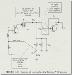
Example 2. Assume that the receiver shown in Fig. 1 2 is being serviced and that the trouble is isolated to the detector. An audio signal injected at the base of Q3 produces a good response on the loudspeaker, as shown in Fig. 1 45. However, no response is obtained when an IF signal modulated by an audio frequency is injected at transformer T4 . Or using signal tracing, an oscilloscope connected across the secondary winding of T4 shows that an AF modulated signal is available to the detector but that no AF signal appears at the base of Q2 .
The detector CR 2 has two outputs: an AF signal and an AVC voltage. Under no signal conditions (i.e., no broadcast signal present), electrons flow through R9 and R8 to ground, producing approximately —1 V bias at the junction of R5 and R9 . With a normal signal being received, electrons flow through Rs and CR2 . This flow (opposite to that produced under no signal conditions) opposes the no signal bias and produces approximately V at the junction of R5 and R9 . This tends to reduce the gain of Q2 (apnp transistor) and thus tends to offset the signal passing through the IF stages.
The amount of AVC voltage is usually not critical, but the fact that the AVC voltage changes with changes in the IF signal is important. The function of the AVC circuit can be checked by measuring the voltage on the AVC line with and without a signal applied to TA . If there is a change of approximately 1 V with signal, the AVC function and detector CR2 can be considered normal.
With CR 2 established as normal but with no signal at the base of Q3 , volume control R l0 or coupling capacitor CM are logical suspects; they are probably open or have broken leads. Capacitor C12 can also be a possible suspect, but it is not as likely as C x , or R 10 . If C12 is shorted or leaking, this will show up in an abnormal voltage (a large negative voltage on the AVC line). If C12 is open, the frequency response characteristics of the audio circuit will be poor, but there will still be a signal at the base of Q3 .
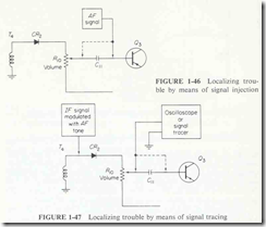
The condition of C x , can be checked in two ways (without removal from the circuit). First, as shown in Fig. 1 46, a signal (audio frequency) can be injected on both sides of Cn . If the signal is heard on the loudspeaker when injected at the base of Q3 but is not heard when injected at the junction of R l0 and Cn , capacitor Cu is probably defective. Second, as shown in Fig. 1 47, a signal can be injected ahead of the detector and traced on both sides of Cn (with an oscilloscope or signal tracer). The signal should appear substantially the same on both sides of Cn . If not, Cn is probably defective.
The condition of R 1 0 can also be checked by signal tracing or signal injection. However, as a final test, the power should be removed and the resistance of R 10 measured. To measure potentiometer resistance, connect the ohmmeter from the wiper arm to one end of the winding, as shown in Fig. 1 48. Then, vary the control from one extreme to the other. Repeat the test with the ohmmeter connected from the wiper arm to the opposite end of the winding. The resistance indication should vary smoothly, with no jumps or flicking of the ohmmeter needle (or jitters of the display if a digital ohmmeter is used). Such jumps can mean bad spots (open or poor contact) on the potentiometer winding.
