Linearity
Bipolar Transistors
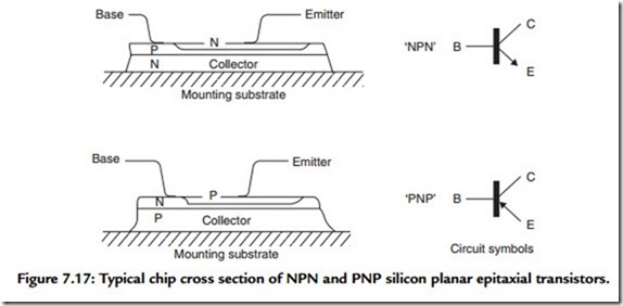
In the case of a normal bipolar (NPN or PNP) silicon junction transistor, for which the chip cross section and circuit symbol are shown in Figure 7.17, the major problem in
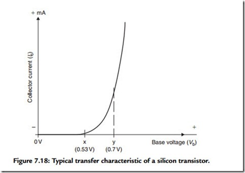
obtaining good linearity lies in the nature of the base voltage/collector current transfer characteristic, shown in the case of a typical “NPN” device (a “PNP” device would have a very similar characteristic, but with negative voltages and currents) in Figure 7.18.
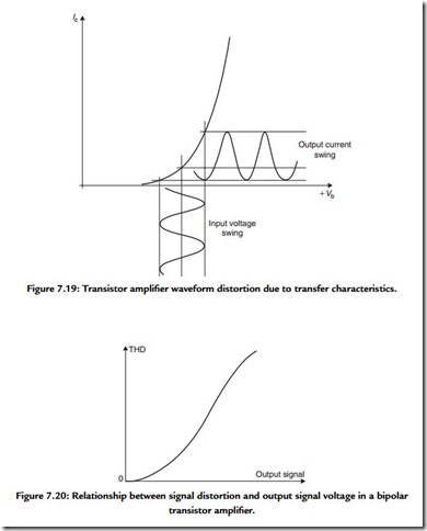
In this, it can be seen that the input/output transfer characteristic is strongly curved in the region “X–Y” and that an input signal applied to the base of such a device, which is forward biased to operate within this region, would suffer from the very prominent (second harmonic) waveform distortion shown in Figure 7.19.
The way this type of nonlinearity is influenced by the signal output level is shown in Figure 7.20. It is normally found that the distortion increases as the output signal increases, and conversely.
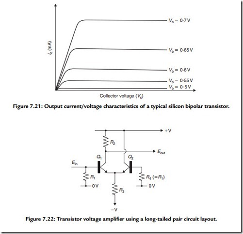
There are two major improvements in the performance of such a bipolar amplifier stage that can be envisaged from these characteristics. First, because the nonlinearity is due to the curvature of the input characteristics of the device—the output characteristics, shown in Figure 7.21, are linear—the smaller the input signal that is applied to such a stage, the lower the nonlinearity, so that a higher stage gain will lead to reduced signal distortion
at the same output level. Second, the distortion due to such a stage is very largely second harmonic in nature.
This implies that a “push–pull” arrangement, such as the so-called “long-tailed pair” circuit shown in Figure 7.22, which tends to cancel second harmonic distortion components, will greatly improve the distortion characteristics of such a stage.
Also, because the output voltage swing for a given input signal (the stage gain) will increase as the collector load (R2 in Figure 7.22) increases, the higher the effective
impedance of this, the lower the distortion that will be introduced by the stage, for any given output voltage signal.
If a high value resistor is used as the collector load for Q1 in Figure 7.22, either a very high supply line voltage must be applied, which may exceed the voltage ratings of the devices, or the collector current will be very small, which will reduce the gain of the device and therefore tend to diminish the benefit arising from the use of a higher value load resistor.
Various circuit techniques have been evolved to circumvent this problem by producing high dynamic impedance loads, which nevertheless permit the amplifying device to operate at an optimum value of collector current. These techniques are discussed later.
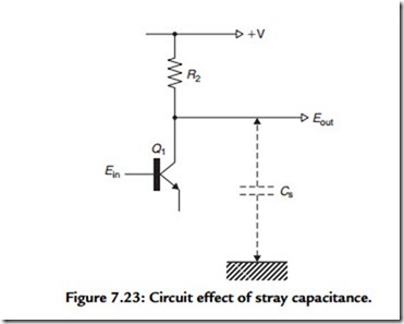
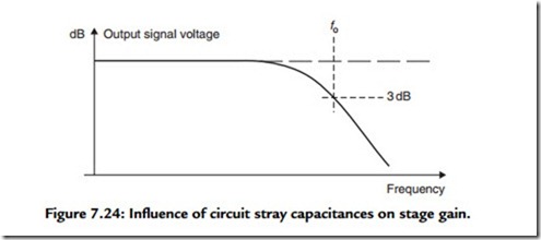
An unavoidable problem associated with the use of high values of collector load impedance as a means of attaining high stage gains in such amplifier stages is that the effect of “stray” capacitances, shown as Cs in Figure 7.23, is to cause the stage gain to decrease at high frequencies as the impedance of the stray capacitance decreases and progressively begins to shunt the load. This effect is shown in Figure 7.24, in which the “transition” frequency, fo (the –3-dB gain point) is that frequency at which the shunt impedance of the stray capacitance is equal to that of the load resistor, or its effective equivalent, if the circuit design is such that an “active load” is used in its place.
Field Effect Devices
Other devices that may be used as amplifying components are field effect transistors and MOS devices. Both of these components are very much more linear in their transfer characteristics but have a very much lower mutual conductance (Gm).
This is a measure of the rate of change of output current as a function of an applied change in input voltage. For all bipolar devices, this is strongly dependent on collector current and is, for a small signal silicon transistor, typically of the order of 45 mA/V per mA collector current. Power transistors, operating at relatively high collector currents, for which a similar relationship applies, may therefore offer mutual conductances in the range of amperes/volt.
Because the output impedance of an emitter follower is approximately 1/Gm, power output transistors used in this configuration can offer very low values of output impedance, even without externally applied negative feedback.
All field effect devices have very much lower values for Gm, which will lie, for small- signal components, in the range 2–10 mA/V, not significantly affected by drain currents. This means that amplifier stages employing field-effect transistors, although much more linear, offer much lower stage gains, with other things being equal.
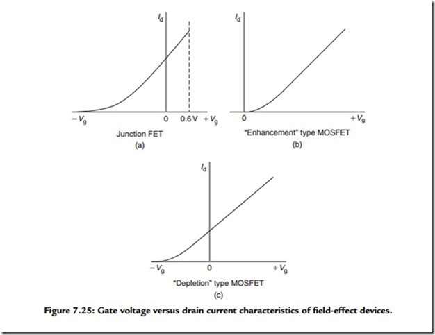
The transfer characteristics of junction (bipolar) FETs, and enhancement and depletion mode MOSFETS are shown in Figure 7.25.
Metal–Oxide–Semiconductor Field-Effect Transistors
Metal–oxide–semiconductor field-effect transistors, in which the gate electrode is isolated from the source/drain channel, have very similar transfer characteristics to that of junction FETs. They have an advantage that, since the gate is isolated from the drain/source channel by a layer of insulation, usually silicon oxide or nitride, no maximum forward gate voltage can be applied—within the voltage breakdown limits of the insulating layer. In a junction FET the gate, which is simply a reverse biased PN diode junction, will conduct if a forward voltage somewhat in excess of 0.6 V is applied.
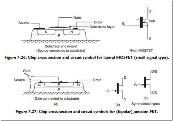
The chip constructions and circuit symbols employed for small signal lateral MOSFETs and junction FETs (known simply as FETs) are shown in Figures 7.26 and 7.27.
It is often found that the chip construction employed for junction FETs is symmetrical, so that the source and drain are interchangeable in use. For such devices the circuit symbol shown in Figure 7.27(c) should be used properly.
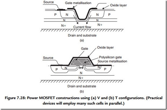
A practical problem with lateral devices, in which the current flow through the device is parallel to the surface of the chip, is that the path length from source to drain, and hence the device impedance and current carrying capacity, is limited by the practical problems of defining and etching separate regions that are in close proximity during the manufacture of the device.
V-MOS and T-MOS
This problem is not of very great importance for small signal devices, but is a major concern in high current ones such as those employed in power output stages. It has led to the development of MOSFETs in which the current flow is substantially in a direction that is vertical to the surface and in which the separation between layers is determined by diffusion processes rather than by photolithographic means.
Devices of this kind, known as V-MOS and T-MOS constructions, are shown in Figure 7.28.
Although these were originally introduced for power output stages, the electrical characteristics of such components are so good that these have been introduced, in smaller power versions, specifically for use in small signal linear amplifier stages. Their major advantages over bipolar devices, having equivalent chip sizes and dissipation ratings, are their high input impedance, their greater linearity, and their freedom from “hole storage” effects if driven into saturation.
These qualities are increasingly attracting the attention of circuit designers working in the audio field, where there is a trend toward the design of amplifiers having a very high intrinsic linearity rather than relying on the use of negative feedback to linearize an otherwise worse design.
Breakdown
A specific problem that arises in small signal MOSFET devices is that, because the gate- source capacitance is very small, it is possible to induce breakdown of the insulating
layer, which destroys the device, as a result of transferred static electrical charges arising from mishandling.
Although widely publicized and the source of much apprehension, this problem is actually very rarely encountered in use, as small signal MOSFETs usually incorporate protective zener diodes to prevent this eventuality, and power MOSFETs, where such diodes may not be used because they may lead to inadvertent “thyristor” action, have such a high gate-source capacitance that this problem does not normally arise.
In fact, when such power MOSFETs do fail, it is usually found to be because of circuit design defects, which have either allowed excessive operating potentials to be applied to the device, or have permitted inadvertent VHF oscillation, which has led to thermal failure.
