Series Regulator Layouts
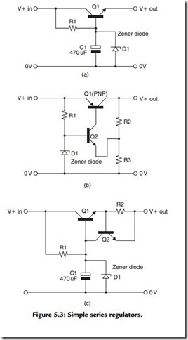
The problem with the shunt regulator arrangement is that the circuit must draw a current that is always greater than would have been drawn by the load on its own. This is an acceptable situation if the total current levels are small, but this would not be tolerable if high output power levels were involved. In this situation it is necessary to use a series regulator arrangement, of which some simple circuit layouts are shown in Figure 5.3.
The circuit of Figure 5.3(a) forms the basis for almost all of this type of regulator circuit, with various degrees of elaboration. Essentially, it is a fixed voltage source to which an emitter–follower has been connected to provide an output voltage (that of the Zener diode less the forward emitter bias of Q1) at a low output impedance. The main problem is that for the circuit to work, the input voltage must exceed the output voltage—the difference is termed the drop-out voltage—by enough voltage for the current flow through R1 to provide the necessary base current for Q1 and also enough current through D1 for D1 to reach its reference voltage. Practical considerations require that R1 shall not be too small. In a well-designed regulator of this kind, such as the 78xx series voltage regulator IC, the drop-out voltage will be about 2 V.
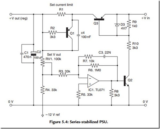
This drop-out voltage can be reduced by reversing the polarity of Q1, as shown in Figure 5.3(b), so that the required base input current for Q1 is drawn from the 0-V rail. This arrangement works quite well, except that the power supply output impedance is much higher than that of Figure 5.3(a), unless there is considerable gain in the NFB control loop. In this particular instance Q2 will conduct and feed current into the Q1 base until the voltage developed across R3 approaches the voltage on the base of Q2, when both Q2 and Q1 will be turned off. By augmenting Q2 with an op-amp, as shown in Figure 5.4, a very high performance can be obtained from this inverted type of regulator layout.

