Diodes are the simplest type of semiconductor. They allow current to flow in only one direction. The knowledge of semiconductors that is acquired by studying diodes is also applicable to other types of semiconductor devices.
P–N Junctions
When pure or intrinsic semiconductor material is doped with a pentavalent or trivalent material, the doped material is called N- or P-type based on the majority carrier. The electrical charge of each type is neutral because each atom contributes an equal number of protons and electrons.
Independent electrical charges exist in each type of semiconductor material, because electrons are free to drift. The electrons and holes that drift are referred to as mobile charges. In addition to the mobile charges, each atom that gains an electron has more electrons than protons and assumes a negative charge. Similarly, each atom that loses an electron has more protons than electrons and therefore assumes a positive charge. As described in Chapter 10, these individual charged atoms are called negative and positive ions. There is always an equal number of mobile and ionic charges within N-type and P-type semiconductor materials.
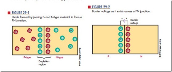
A diode is created by joining N- and P-type mate- rials together (Figure 29-1). Where the materials come in contact with each other, a junction is formed. This device is referred to as a junction diode.
When the junction is formed, the mobile charges in the vicinity of the junction are strongly attracted to
their opposites and drift toward the junction. As the charges accumulate, the action increases. Some elec- trons move across the junction and fill some of the holes near the junction in the P-type material. In the N-type material, the electrons become depleted near the junction. This region near the junction where the electrons and holes are depleted is called the depletion region, which extends only a short distance on either side of the junction.
There are no majority carriers in the depletion region, and the N-type and P-type materials are no longer electrically neutral. The N-type material takes on a positive charge near the junction, and the P-type material takes on a negative charge.
The depletion region does not get larger. The combining action tapers off quickly, and the region remains small. The size is limited by the opposite charges that build up on each side of the junction. As the negative charge builds up, it repels further electrons and keeps them from crossing the junc- tion. The positive charge absorbs free electrons and aids in holding them back.
These opposite charges that build up on each side of the junction create a voltage, referred to as the barrier voltage. It can be represented as an external voltage source, even though it exists across the P–N junction (Figure 29-2).
The barrier voltage is quite small, measuring only several tenths of a volt. Typically, the barrier voltage is 0.3 V for a germanium P–N junction and 0.7 V for silicon P–N junction. This voltage becomes apparent when an external voltage source is applied.
Questions
1. Define the following terms:
a. Donor atom
b. Acceptor atom
c. Diode
2. What occurs when an n-type material is joined with a P-type material?
3. How is the depletion region formed?
4. What is the barrier voltage?
5. What are typical barrier voltages for germanium and silicon diodes?
