Electronic Circuits: Digital
Practically Everything Is Digital These Days
In this Chapter:
● Binary number system.
● Logic gates and flip-flops.
● Common combinational and sequential circuits.
● Semiconductor memory.
● Programmable logic devices.
● Analog-to-digital and digital-to-analog conversion.
INTRODUCTION
Recall that there are two basic types of electronic signals—analog and digital. A digital signal is one that varies in discrete steps. Unlike an analog signal, which varies continuously, a digital signal has two levels or states. The signal switches or changes abruptly from one state to the other.
Figure 5.1 shows a DC digital signal that switches between two known lev- els such as zero volts or close to it (<0.1 volt) or 0 V and +3.3 V. The positive voltage can be anything between about 1 volt and 12 volts with 3.3 and 5 being the most common.
Digital signals with two discrete levels are also referred to asbinary signals.
Binary means two—two states or two discrete levels of voltage.
Humans use the decimal number system that represents quantities with digits 0 through 9. However, digital equipment and computers do not. Internally, digital equipment processes binary data.
BINARY NUMBERS
The binary number system is a set of rules and procedures for representing and processing numerical quantities in digital equipment. Because the base of the binary number system is 2, only two symbols (0 and 1) are used to represent any quantity. The symbols 0 and 1 are called binary digits or bits. For example, the 6-bit number 101101 represents the decimal number 45. Your understand- ing of how digital circuits, microprocessors, and related equipment process data is tied directly to an understanding of the binary number system.
The reason for using binary numbers in digital equipment is the ease with which they can be implemented. The electronic components and circuits used to represent and process binary data must be capable of assuming two discrete states to represent 0 and 1. Examples of two-state components are switches and transistors. When a switch is closed or on, it can represent a binary 1. When the switch is open or off, it can represent a binary 0. A conducting transistor may represent a 1, whereas a cut-off transistor may represent a 0. The representa- tion may also be voltage levels. For example, a binary 1 may be represented by
+3.3 V and a binary 0 by 0 V as previously shown in Figure 5.1.
Binary-to-Decimal Conversions
The binary system is similar to the decimal system in that the position of a digit in a number determines its weight. Recall that in the decimal system the weights are powers of 10. The right-most digit is units or 1’s, and then 10’s, 100’s, 1000’s, and so on, moving from right to left from one digit to the next. The position weights of a binary number are powers of 2:
20 = 1
21 = 2
22 = 4
23 = 8
24 = 16
25 = 32
26 = 64
27 = 128
28 = 256
The position weights of an 8-bit binary number follow:
The most significant digit or bit (MSB) and the least significant bit (LSB) are identified.Now let’s evaluate the decimal quantity associated with a given binary number, 101101. You simply multiply each bit by its position weight and add the values to get the decimal equivalent, 45.
1 X 1 = 1
0 X 2 = 0
1 X 4 = 4
1 X 8 = 8
0 X 16 = 0
1 X 32 = 32
Decimal 45
equivalent
You can see that positions with a 0 bit have no effect on the value. Therefore, they can be ignored. To quickly determine the decimal equivalent of a binary number, simply sum the weights of the positions containing a 1 bit. For example, in the number 11101, the weights of those positions with a 1 bit from right to left are 1 + 4 + 8 + 16 = 29.
Using Hardware to Represent Binary Quantities
Switches are widely used to enter binary data into computers and digital equip- ment. If the switch is set to the up position, a binary 1 is represented. If the switch is down, a binary 0 is represented. The switch contacts can be open or closed depending on the circuit in which the switch is connected. Figure 5.2 shows a group of slide switches set to represent a binary number, 11000101 or 197.
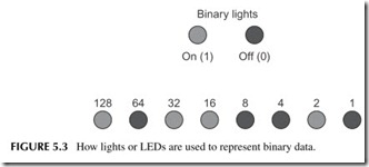
Indicator lights such as light-emitting diodes (LEDs) are sometimes used to read out binary data in digital equipment. An “on” light is a binary 1 and an “off” light is a binary 0. See Figure 5.3. The decimal value being represented by the display is 178.
Decimal-to-Binary Conversions
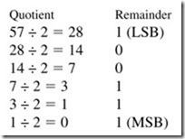
You may find it necessary to convert decimal numbers into their binary equiv- alents. This can be done by dividing the decimal number by 2, dividing the quotient by 2, dividing that quotient by 2, and so on, recording the remainders until the quotient is zero. The remainders form the binary equivalent.
In the following example, we convert the decimal number 57 to its binary equivalent.
You can always check your work by reconverting the binary number back to decimal using the procedure described earlier. Also, keep in mind that some sci- entific calculators can do binary-to-decimal and decimal-to-binary conversions.
Another name for a binary number is binary word. The term word is more general. It refers to a fixed group of bits that can mean numbers, letters, or special characters and codes. We say that digital equipment processes binary data words.
All digital circuits and microcomputers work with a fixed-length binary word. A common binary word length in microcomputers and other digital equipment is 8 bits. All data storage, processing, manipulation, and trans- mission are carried out in 8-bit groups. Word lengths of 4, 8, 12, 16, 32, and 64 bits are common in digital equipment.
An 8-bit word is usually called a byte. In data communication applications, an 8-bit word is sometimes called an octet. A 4-bit word is sometimes referred to as a nibble.
Maximum Decimal Value for N Bits
The number of bits in a binary word determines the maximum decimal value that can be represented by that word. This maximum value is determined with the formula:
M = 2N – 1
where M is the maximum decimal value and N is the number of bits in the word.
For example, what is the largest decimal number that can be represented by 4 bits?
M = 2N – 1 = 16 – 1 = 15
With 4 bits, the maximum possible number is binary 1111, or decimal 15.
The maximum decimal number that can be represented with 1 byte is 255 or 11111111. An 8-bit word greatly restricts the range of numbers that can be accommodated. But this is usually overcome by using larger words.
There is one important point to know before you leave this subject. The formula M = 2N – 1 determines the maximum decimal quantity (M) that can be represented with a binary word of N bits. This value is 1 less than the maxi- mum number of values that can be represented. The maximum number of val- ues that can be represented (Q) is determined with the formula:
Q = 2N
With 8 bits, the maximum number of values is 256 or 0 through 255.
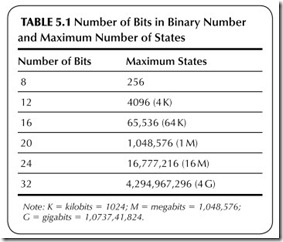
Table 5.1 gives the number of bits in a binary number and the maximum number of states that can be represented.
BCD and ASCII
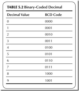
The binary numbers we have been discussing are usually referred to as pure binary codes. But there are other types of binary codes. For example, the binary-coded decimal (BCD) system is popular. BCD is a hybrid code between the binary and decimal systems. It was developed in an attempt to simplify the conversion processes between the two systems and to improve human–machine communication.
To represent a decimal number in the BCD system, each digit is replaced by its 4-bit binary equivalent. Thus, the number 729 in BCD is:
72 9
0111 0010 1001
The BCD code is given in Table 5.2.
It is important to note that the 4-bit binary numbers 1010 through 1111 that represent the decimal values 10 through 15 are invalid in BCD.
To convert a BCD number to decimal, simply substitute the decimal equivalent of each 4-bit group. The BCD number 1001 0100 0110 in decimal is 946.
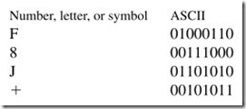
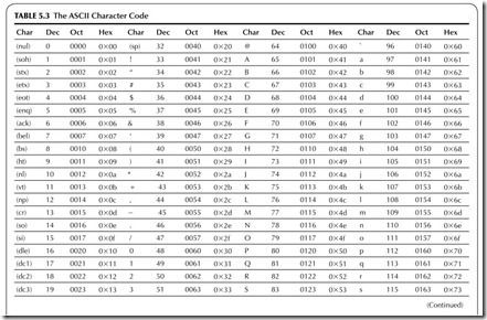
A special form of BCD code is used in computers and data communica- tions systems. It is a 7- or 8-bit code that is used to represent not only numbers but also letters (both uppercase and lowercase), special symbols, and control functions. This code is called the American Standard Code for Information Interchange, or ASCII (pronounced “ask-key”).
The following are examples of ASCII:
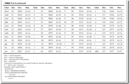
The complete ASCII is given in Table 5.3. It provides the decimal and hexadecimal (hex) values of the codes. The code contains both uppercase and
lowercase letters, the digits 0 through 9, punctuation marks, common math- ematical symbols, and many special two- and three-letter codes. The special codes are known as control codes. They are used to indicate the start and end of a string of characters or to initiate special operations. Some examples follow:
STX—Start of text sequence
EOT—End of transmission of a string of characters BEL—Ring a bell
DEL—Delete LF—Line feed CR—Carriage return
These codes not only represent alphanumeric data but can also make things happen in a printer or computer.
The main use of ASCII is in data communication. Computers use ASCII to “talk” to their peripheral units, such as printers, or to one another. A com- mon example is a personal computer that receives data via a modem from the Internet. Another example is the data sent from a computer to a laser printer. ASCII is the communication code for text.
Hexadecimal Notation
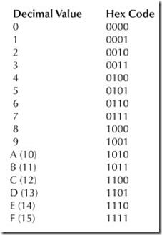
Hexadecimal notation is a way to represent binary values with numbers and letters in an effort to make data easier to remember, and to reduce the errors normally associated with writing or reading long strings of 1’s and 0’s. The hex code is just an extension of the BCD code, with the decimal values from 11 to 15 represented by the letters A through F. See the following table.
Hexadecimal Notation (Continued)
As an example to convert the binary number 101000110101100 to hex, you divide the word into 4-bit groups starting on the right and then replacing each with the hex codes. In this case, the hex code is A35C.
Parallel and Serial Data
It is frequently necessary for digital devices to communicate. Someone using a computer may have to send data to a printer. Or two people using personal com- puters may have to communicate over a local area network (LAN). To accomplish either of these objectives, one must transmit binary data from one circuit to another. This is done in one of two ways: parallel transmission or serial transmission.
Parallel Data
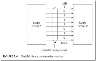
When the parallel method is used, all bits of a binary word or number are transmitted simultaneously. Figure 5.4 shows an 8-bit word being transferred from logic circuit 1 to logic circuit 2.
A bus is a set of parallel data lines over which digital data is transferred. A data bus can have any number of data lines as required by the application. However, the main characteristic of a bus is parallel data transfer. In physical form, a bus is usually implemented on a connector, with lines of copper on a printed circuit board or with a ribbon cable with one wire per bit.
Because all bits are transmitted at the same time over a parallel bus, data movement is extremely fast. The main benefit of parallel data transmission is its high speed. With high-speed logic circuits, a binary word can be transferred from one point to another in as little as several nanoseconds. Parallel data trans- mission over buses in computers takes place at rates up to several hundred meg- ahertz. It is not uncommon to see a rate of 100 million bits per second (Mbps)
on a personal computer data bus. On long buses, data rates are slower because the stray inductance and capacitance of the cable typically distorts the data and slows the transmission speed.
Although parallel transmission is fast, it is expensive, because there must be circuitry for each bit on both the sending and receiving ends. There must be one wire per bit in a cable plus a separate ground wire. This increases the complexity and thereby the cost of the circuitry.
Serial Data
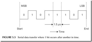
The other method of moving binary data from one point to another is serial transmission. In the serial method, the bits of a word are transmitted one at a time, or sequentially. Figure 5.5 shows the waveform of an 8-bit serial binary word. This is the voltage that you would monitor at the single output of the circuit generating the word. It is the waveform that an oscilloscope would dis- play. Each bit occurs for a fixed time interval such as 1.5 milliseconds. Thus, it takes 1.5 X 8 = 12 milliseconds (ms) to transmit an 8-bit word.
The speed of data transmission is measured in bits per second (bps). That figure can be calculated from the expression:
Here, t is the time for 1 bit. In Figure 5.5, 1 bit takes 1.5 μs. The speed of the data, then, is
bps = 1 -:- (1.5 X 10⁻⁶ ) = 666, 666.7 bps or 666.7 kbps
If you know the speed in bps, you can calculate the bit time (t) by rearranging the formula:
Assume a data rate of 14,400 bps. The bit time is 69.4 μs.
As seen in Figure 5.5, the MSB is transmitted first. Depending on the system used, however, the LSB can be sent first. In any case, the speed of transmission depends on the number of bits in the word and the duration of each bit. It is this longer transmission time that is the primary disadvantage of the serial method. However, although serial transmission is slower than parallel transmission, it is perfectly suitable for many applications. Common data rates are in excess of millions of bits per second. Data rates of more than 10 Gbps are common.
The main benefits of the serial method are its simplicity and low cost. Only a single line rather than multiple lines is needed to interconnect the equipment. In addition, only one set of sending and receiving circuits is needed. All data transmissions by copper cable or fiber optical cable exceeding about 100 Mbps are made by the serial method. All wireless data transmissions are serial.
DIGITAL LOGIC ELEMENTS
Digital logic elements are the basic circuits that are used to process the binary data. The logic element has one or more binary data inputs to be processed. The logic element processes or manipulates the binary input signals in a fixed way and generates an appropriate output signal. The output is a function of the binary states of the inputs and the unique processing capability of the logic element. The logic element “looks” at the binary input signals, and then makes a decision and generates an appropriate output. There are five elementary logic circuits: inverter or NOT, AND, OR, NAND, and NOR. These functions are performed by logic elements known as inverters and gates.
You need not be concerned with the inner workings of these logic elements. Instead, your primary concern is with the basic logic functions. Needless to say, the gates and inverters are inside every microcomputer and digital integrated circuit.
Inverter
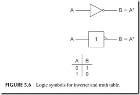
The inverter has a single input and a single output. The logic function per- formed by an inverter is inversion. The output of the inverter is simply the inverse, or opposite, of the input. Because binary signals can assume only one of two different states, either 0 or 1, the inverter generates a 0 when the input is a 1, and a 1 when the input is a 0.
Two common symbols used to represent an inverter are shown in Figure 5.6. The input and output are given names, which are usually letters of the alphabet. There are a variety of ways to express the operation of various logic func- tions. One way is to use Boolean algebraic expressions. A Boolean expres- sion is a simple mathematical or algebraic formula that expresses the output in
terms of the input. The Boolean expression for the inverter is:
B = A*
This equation is read, “B equals not A.” The asterisk means NOT or inversion. What this expression is telling you is that if the input is A, the output, B, is not A.
Another method of expressing the function of a logic element is a truth table. This is simply a table listing all possible combinations of the inputs and outputs of a logic element. Figure 5.6 also shows the truth table for an inverter. There are only two possible inputs, 0 and 1, and the corresponding outputs. A truth table completely defines the operation of a logic element.
AND Gate
A gate is a circuit that has two or more inputs and a single output. The gate generates a binary output that is a function of the states of the inputs and the nature of the gate itself.
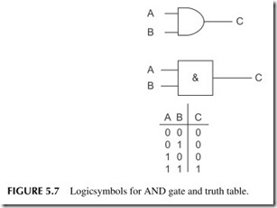
The type of gate determines how the binary inputs are processed. The two basic logic gates are the AND gate and the OR gate. An AND gate is a logic circuit that generates a binary 1 output if all of its inputs are binary 1’s. Otherwise, the circuit generates a binary 0. All of the inputs have to be binary 1 for the AND gated to produce a binary 1 output. If any one of the inputs is a binary 0, the output is binary 0.
Figure 5.7 shows the logic symbols used to represent an AND gate. Letters of the alphabet are used to represent inputs and outputs. There may be more than two inputs, but there is only one output.
As with the inverter, the output of the AND gate can be expressed in terms of the inputs with a Boolean expression. The Boolean expression for an AND gate is:
C = AB
This equation is read, “C equals A and B. ”Parentheses also can be used to separate the inputs; for example, C = (A)(B).
The truth table for a simple two-input AND gate is also shown in Figure 5.7. Note that the output C is a binary 1 when both inputs are binary 1’s. At all other times, the output is binary 0. With two inputs, there are a total of four differ- ent input combinations (22 = 4). With three inputs, there are 23 = 8 possible input combinations for an AND gate. These inputs are the binary numbers 000 through 111.
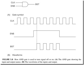
One of the most common applications of an AND gate in digital circuits is gating. Gating simply refers to the use of one binary signal to control another. A two-input AND gate is most often used as a control gate. One input signal is the control that either keeps the other input signal from passing through to the output or allows it to pass.
Figure 5.8 shows the inputs and output of a typical control gate. Note that multiletter names called mnemonics are used instead of single letters to des- ignate the input and output signals. The ENB or enable input represents the control signal. As long as the ENB input is a binary 0, the output is a binary 0. The gate is said to be inhibited because nothing more than a binary 0 output occurs.
When the ENB control input is a binary 1, the gate is enabled. At this time, the main input signal, CLK for clock, is allowed to pass through to the out- put BST. CLK is a periodic clock signal that switches repetitively between the binary 0 and the binary 1 levels at a fixed frequency. The output of the AND gate follows the CLK input as long as the ENB control input is a binary 1.
OR Gate
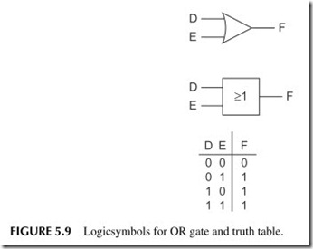
Another commonly used logic gate is the OR circuit. Like the AND gate, the OR gate has two or more inputs and a single output. The OR gate generates a binary 1 if any one or more of its inputs are binary 1. The only time the output of an OR gate is binary 0 is when all its inputs are binary 0.
The symbols used to represent an OR gate are shown in Figure 5.9. Letters of the alphabet are used to designate the inputs and outputs. Using these desig- nations, the Boolean output expression for the OR gate is:
D = E + F
This equation is read, “D equals E or F.” In this Boolean expression, the plus sign designates the OR function. In a Boolean logic expression, the plus sign does not
mean addition. In Figure 5.9, the mathematical symbol> (greater than or equal to) is used to designate the OR logic function. The truth table for an OR gate further defines its operation. The output D is a binary 1 when input E or input F or both are a binary 1. Like an AND gate, an OR gate can have any number of inputs.
NAND and NOR Gates
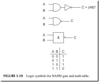
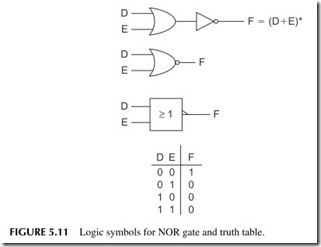
The AND and OR logical functions are basic to all digital systems. Although these functions are implemented with AND and OR gates, a variation of these gates is even more widely used. These are NAND and NOR gates, which are a combination of either an AND gate or an OR gate and an inverter. These gates are more flexible in their application when they are used together.
A NAND gate can be made with an AND gate followed by an inverter. Figure 5.10 shows this circuit configuration. Note the two special symbols in Figure 5.10 used to represent the logical NAND function. The truth table is also given.
A NAND gate can perform all of the gating and detection functions men- tioned earlier for an AND gate. The only difference is that the output is inverted.
The other widely used digital logic element is a NOR gate. A NOR gate is a combination of an OR gate followed by an inverter (see Figure 5.11 ). The symbols used to represent the NOR logic function are also shown. The out- put of a NOR gate is simply the complement of the output of an OR gate, as shown by the truth table. An XOR actually is a 1-bit binary adder.
Exclusive OR Gate
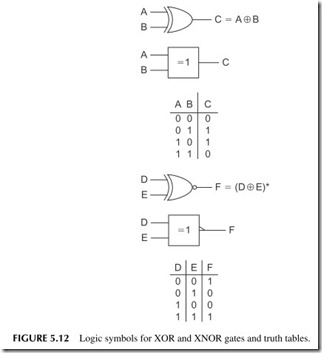
A variation of the OR gate is the exclusive OR, usually designated XOR. Its symbols are given in Figure 5.12. The truth table is also shown. Note that the
circuit only produces a 1 output if the two inputs are opposite. The output is 0 if the two inputs are the same.
An inverted XOR or XNOR has the symbols and truth table shown in Figure 5.12. It is useful as a 1-bit comparator since the output is 1 if both inputs are the same.
Flip-Flops
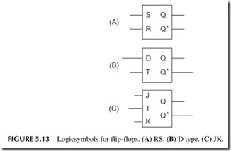
A flip-flop (FF) is another basic building block of electronics. It is essentially a circuit that stores 1 bit of data. The circuit has two states—set and reset. If the FF is storing a binary 1, it is set. If it is storing a binary 0, it is reset. Figure 5.13A shows the basic block diagram of a reset-set (R-S) FF. The inputs are set (S) and reset (R). The two outputs Q and Q* are complementary. You apply an input to the appropriate input to set or reset the FF.
A D-type flip-flop is shown in Figure 5.13B. It has a D or data input and a clock (T) input. When the clock occurs, the FF is either set or reset depending on the value of the D input. The D FF is used to store 1 bit of data.
Another type of FF is the JK, shown in Figure 5.13C. It has J and K inputs that correspond to S and R inputs, respectively. It also has a clock or T input that performs the set or reset operations. To store a binary 1, you make J = 1 and K = 0. When a clock input occurs, the FF is then set or reset.
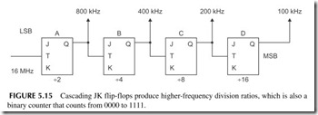
The T input also causes the state of the FF to toggle or change state when a clock transition occurs (see Figure 5.14 ). This feature is used to produce fre- quency division by 2 as shown. The output is a square-wave half the frequency of the T input. Additional JK FFs can be cascaded to produce frequency division by the power of 2 or 2, 4, 8, 16, 32, 64, and so on, as shown in Figure 5.15.
Storage Registers
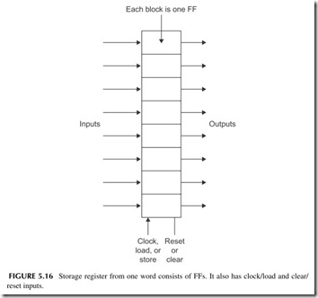
A storage register is a place to store a binary word or number. It is made up of 1 FF per bit. An 8-bit register stores bytes and has 8 FFs. Figure 5.16 shows a register with eight inputs and eight outputs. Most registers also have a clock input also called LOAD or STORE that determines when the input data is stored. Some also have a CLEAR or RESET input that puts all the FFs in the binary 0 state.
Shift Registers
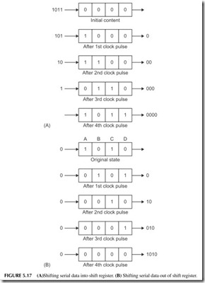
A shift register (SR) is like a storage register, but the bits stored there may be shifted from one FF to the next as each clock pulse occurs. Figure 5.17A shows how serial binary data is shifted into the SR for storage. As new data
is shifted in, the existing data will be shifted out and sent to another circuit. Figure 5.17B shows data being shifted out as binary 0’s are shifted in.
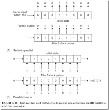
Shift registers are often used for parallel-to-serial and serial-to-parallel conversions. A serial-to-parallel conversion is shown in Figure 5.18A. The SR initially contains all binary 0’s. Then serial data is shifted in and the output is taken in parallel from the FF outputs. For parallel-to-serial conversion, a binary word is initially stored in the register. Then the word is shifted out as the clock pulses occur (see Figure 5.18B).
Counters
As its name implies, a counter is a circuit that counts input pulses. Counters are made of multiple cascaded FFs, and they are sometimes accompanied by logic gates. As the input pulses occur, the binary number stored in the coun- ter FFs tells how many pulses have occurred. The frequency divider shown in Figure 5.15 is also a 4-bit counter. It can count from 0 (0000) to 15 (1111).
If all FFs are initially reset to 0, then 10 pulses occur, and the FFs from A to D would be storing 0101 from left to right. The right-most FF (D) is the MSB, so you read the counter as 1010 or the binary equivalent of decimal 10.
Binary counters can store numbers up to 2N – 1, where N is the number of FFs. For example, an 8-bit counter would count from 00000000 to 11111111 or 28 – 1 = 256 – 1 = 255.
Figure 5.19 shows a counter where 178 pulses have occurred, so the coun- ter stores the number 10101011 that is the binary equivalent of 179.
Another popular form of counter is the BCD version that counts from 0000 to 1001 or 0 through 9. BCD counters are used to keep track of decimal quan- tities in binary form. BCD counters can serve as frequency dividers as well. Each divides by 10.
COMMON LOGIC CIRCUITS
There are several types of logic circuits that occur again and again in digital equipment. The counters and registers just described are good examples. A few others that you may encounter are described in this section. Remember that these circuits can be made from individual gates and FFs in IC form. You can also buy them in IC form already wired for their specific function. But mostly these circuits appear as a collection of circuits inside some larger IC.
Multiplexer
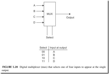
A multiplexer or mux is a circuit with two or more inputs and one output (see Figure 5.20). Here there are four inputs and one output. Two other inputs are used to select one of the inputs to appear as the output. The four selected inputs are 00, 01, 10, and 11. In the figure, note which input is routed to the output with each input select code. Multiplexers can have as many inputs as needed.
Demultiplexer
A demultiplexer or demux is the opposite of a mux. It has one input and mul- tiple outputs. Like the mux, select inputs specify which of the output lines the input is connected to.
Decoder
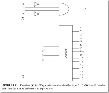
A decoder is a circuit that can detect a specific binary code. In its simplest form, it is just an AND gate, as shown in Figure 5.21A. If the input 0110 appears at the inputs, the AND gate will have all its inputs at binary 1, so the output will be binary 1 indicating that it is detecting the desired input. For any other 4-bit input, the output will be binary 0.
Decoders can also be made to detect all states of a given binary input. For example, a 4-bit decoder like that in Figure 5.21B looks at the 4-bit inputs and decodes all states from 0000 to 1111. If the input is 1000, the 8 output is binary 1 and all other outputs are 0.
Comparators
A comparator takes two binary words as inputs and compares them. If the two inputs are equal, a binary 1 output occurs. Otherwise, if the two inputs are dif- ferent, the output is 0. Some comparators have outputs that can tell if one input is larger than or smaller than the other.
Arithmetic Circuits
Digital logic does a good job of basic arithmetic functions like add and sub- tract. The basic computing element is called an arithmetic logic unit (ALU). It does binary addition and subtraction. It can also perform basic logic operations such as AND, OR, or XOR on two binary input words. Circuits for multiplica- tion and division are more complex, but are common in digital computers.
DIGITAL MEMORIES
Digital memories are semiconductor circuits that store binary data. You have probably heard of the terms RAM and ROM as they apply to personal comput- ers. These are the two main types of memory, random access memory (RAM), and read-only memory (ROM).
RAM
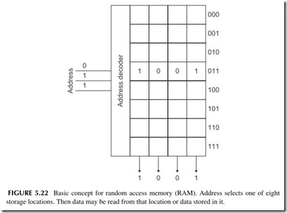
The random access memory is one in which you can access hundreds, thou- sands, or millions of binary storage locations. You can store one binary number or word in each location or read the data out of the location. Each location is referred to by a unique binary number called the address. You send the mem- ory an address and activate the selected location. Then you can read data from the location or write data into that location. RAMs therefore are what we call read-write memories.
Figure 5.22 shows the concept of a RAM. It has eight locations for 4-bit words. To address eight locations you need a 3-bit address (23 = 8). When you apply the address to the address decoder, the decoder activates the desired location. In the figure you see that the binary number 1001 stored in location 011 is being accessed and read out.
Most memories are large today. We talk about megabytes (MB) or millions of bytes of data or gigabytes (GB) or billions of bytes of data in a modern PC. Embedded controllers will have fewer locations, usually in the thousands of bytes (KB) or perhaps more in the larger systems. Storage word sizes are usu- ally 8 (bytes), 16, 32, or 64 bits.
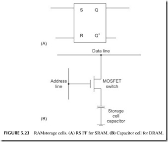
There are two ways to make a RAM. The first way is just to build one FF for each bit to be stored. The basic set-reset FF described earlier is the basic storage circuit (see Figure 5.23A ). Memories using this type of circuit are called static RAM or SRAM. They are called static because once you store the bit in the FF, it stays there as long as power is applied to the circuit.
The other form of RAM is called dynamic RAM or DRAM. The basic stor- age circuit is a capacitor as shown in Figure 5.23B. If you charge the capaci- tor, it is storing a binary 1. If the capacitor is discharged, a binary 0 is being stored. A MOSFET is used as a switch to access the capacitor. If the MOSFET is turned on by an input address on the gate, it connects the capacitor to the data line, where it may be read out or where a new bit may be stored. When the MOSFET is turned off, the capacitor is isolated and just stores the bit.
The reason why the termdynamic is used for this type of RAM is that the charge on the capacitor will leak off very quickly. The capacitor is very small and millions of them are made on a tiny chip of silicon. For this reason, the capacitor has to be recharged every so often so that the data is retained. This is called a refresh operation and it usually occurs every 2 milliseconds or so.
Comparing SRAM and DRAM, you should know that SRAM is the faster of the two in that you can store data or read data out faster than you can with a
DRAM. The downside is that the SRAM is more complex and takes up more space on the chip, and thus costs more. The DRAM is slower but not much. Its advantage is that you can put more storage cells on a chip, making them cheaper. The need to refresh is a downside but easy to live with, as all the refresh circuitry is on the chip and the process is transparent to the user.
Just keep in mind a key fact. RAM is fast and reliable, but it loses all data if the DC power to the memory circuit is removed. All data is erased. RAMs are therefore said to be volatile.
ROM
Read-only memories are nonvolatile memories. Once you store data in them, they retain the data when power is removed. In some ROMs, you can change the data stored there. Incidentally, all ROMs are random access in that you can go to any desired location to read or maybe write data.
There are several categories of ROM. The older types are called masked ROM, where the mask refers to the actual wiring of the ROM to permanently fix the data in the circuitry when it is made. The storage cells are essentially a MOSFET matrix where each MOSFET is permanently turned on or off to store 1 or 0. No changes are possible. Later a programmable ROM or PROM was developed. It used a special MOSFET that could be programmed on or off. You could then erase the programming by shining ultraviolet (UV) light
on the chip for a short time. Then the PROM could be reprogrammed. These are no longer used.
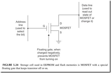
Most ROMs today are what we call electrically erasable programmable ROMs or EEPROMs or E2 PROMs. The storage element is a MOSFET that you turn off or on with a programmable voltage (see Figure 5.24 ). The MOSFET retains that state until it is electrically changed.
The main problem with EEPROMs is that they are slow to erase and repro- gram. But today we have a special version of EEPROMs called flash memo- ries. These are also EEPROMs, but they actually are almost as fast as RAMs for reading and writing data. Yet they are nonvolatile.
You will hear of two types of flash memory—NOR and NAND. NOR flash is used to store programs for microcontrollers. It can only be erased on large block sizes and not individual cells. NAND flash is faster and you can erase individual memory locations. The NAND flash is gradually replacing the NOR flash in many applications.
Flash memory has become so popular it is used in almost every electronic product today. MP3 players and iPods store music in flash memory. Cell phones store phone numbers, digital cameras store photos, and in embedded controllers, the flash usually stores the program that tells the processor what to do. And, let’s not forget the flash drive or “thumb” drive as it is called. These devices with a USB connector can store many gigabytes of data and are very inexpensive. Flash memory is also used to make solid-state drives (SSDs) that are the equivalent of the hard disk drives used in PCs and laptops. They are still expensive, but as prices decline, you can look for more SSDs to replace conventional mechanical/magnetic hard drives.
PROGRAMMABLE LOGIC DEVICES
There are two ways that digital devices are built today. The most common is to use an embedded controller or microcomputer. This is a single-chip computer that you can program to do whatever digital function you want. Most electronic products have at least one embedded controller at the heart of their design.
In some cases, the embedded controller is not fast enough to do the job. One way to make the circuitry is to use individual logic circuits such as gates, flip-flops (FFs), counters, and so on. That is the way it used to be done. Now, if you need fast custom digital logic, you build the circuit with a programma- ble logic device (PLD). A PLD is an IC that contains a mix of gates, FFs, and other circuits that can be programmed to implement any digital function. The programming is usually done on a computer and a file is created. The file is then downloaded to the PLD, where it is stored in a RAM or ROM. The file in the memory determines how the unique circuit is formed.
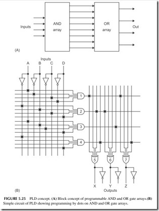
There are three basic types of PLDs: simple PLDs, complex PLDs, and field programmable gate arrays (FPGAs). The SPLDs are small devices for simpler digital circuits. The most common types are called programmable array logic (PAL), programmable logic arrays (PLAs), and generic array logic (GAL). PROMs are also used as SPLDs. For example, the address input to a ROM is some binary number or a collection of binary inputs. These form an address to locate a specific binary word stored in that location. When that par- ticular selection of input bits occurs, it forms the address that identifies the memory location where the desired set of output responses is stored. This form of SPLD is also called a look-up table or LUT.
The other SPLDs are essentially a set of AND and OR gates that can be pro- grammed. They all take the form shown in Figure 5.25. You can select which inputs go to the AND gates, and/or select which AND outputs go to which OR gate inputs. A PROM has the AND array fixed and you can program the OR gates. A PAL is an SPLD in which you can program the AND inputs but the OR connections are fixed. A PLA is a PLD that lets you program both the AND inputs and the OR connections. In both PLAs and PALs, the programming is usually permanent.
A GAL is a variation of the PAL with its AND inputs programmable. The difference is that the programming can be changed. The program you develop is actually stored in flash memory. The flash memory cells send the program- ming bits to the various AND and OR gates telling them what logic to imple- ment. You can then erase it and reprogram if you want or need to. GALs also have one or more FFs associated with the logic gates, so you can store bits or actually build counters and registers by programming.
CPLDs are complex PLDs similar to SPLDs, only larger. They contain more gates and flip-flops so that very large logic projects can be built on a single chip. A typical CPLD is really just a large collection of PALs or GALs that can be individually programmed and then connected together with a large
interconnect matrix. Input/output (I/O) circuits also provide inversion if needed or extra power to drive external circuits. Again, flash memory is used to store the programming.
The largest and most flexible PLD is the field programmable logic array or FPGA. It has become the most popular and common way to implement dig- ital equipment other than a microcontroller. FPGAs are large chips that contain
thousands of logic circuits. The largest devices have millions of gates and other circuits. Most FPGAs are programmed by storing a bit pattern in the SRAM cells inside. These cells tell the logic circuits what configuration to take and what functions to perform. If you turn the power off, the programming goes away and all you have is a dumb FPGA with no logic interconnections or func- tions. When you power up an FPGA, the desired program, usually from a flash memory, or a computer loads the RAM cells with the program, thereby enabling the FPGA to perform its desired function.
The logic inside an FPGA is essentially thousands of look-up tables (LUTs) that can be individually programmed. Each LUT has its own program memory block as well as one or more FFs and I/O circuits. The LUTs may also be interconnected to one another by programming. With this arrangement virtually any digital logic operation can be programmed. You can even make your own custom computer with an FPGA, for example.
There are about a half-dozen companies that make PLDs. The two oldest and largest are Xilinx and Altera. Both have extensive lines of CPLDs and FPGAs.
DATA CONVERSION
The term data conversion refers to the translation of analog signals into digital form and vice versa. While it used to be an all-analog electronics world, today it is virtually all digital. We still have analog signals such as voice, video, radio waves, and sensor voltages, but mostly we process, store, and transmit data by digital means. For that reason, circuits that perform these conversions are criti- cal to virtually all electronic applications. All cell phone voice is digital, all modern TV is digital, and sensor outputs are captured and processed in digital form. It is difficult to name a product today that does not use some form of data conversion.
Analog-to-Digital Conversion
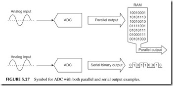
The process of converting an analog signal into a digital one is called analog- to-digital conversion, and it is performed by an analog-to-digital converter (ADC). The process, also referred to as sampling, is illustrated in Figure 5.26. The ADC looks at the analog input and periodically takes a sample of the volt- age at that instant, captures it, and then converts it into a proportional binary number. We say that we are digitizing the signal. The sample points are shown by the dots on the analog curve. The binary value of the sample is shown to the right of the curve. The conversion process actually results in a sequence of binary numbers that represent the analog waveform. These values are usually stored in a RAM or transmitted to other circuits as shown in Figure 5.27. Note the symbol for an ADC.
Digital-to-Analog Conversion
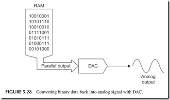
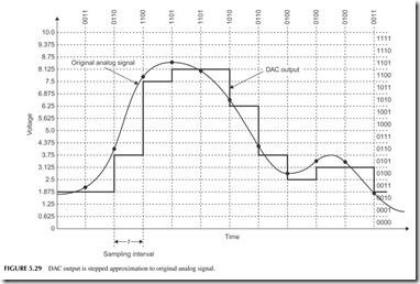
To recover the original signal, we put the data sequence previously captured by the ADC into a digital-to-analog-converter (DAC) (see Figure 5.28). The out- put is a version of the analog signal. The DAC output is not a perfect reproduc- tion, but just an approximation. This is shown in more detail in Figure 5.29. Each binary input results in a constant voltage output from the DAC during the sample period. The result is a stepped approximation to the original signal. The rate at which the binary data is sent to the DAC must be the same as the sampling interval to recover the original frequency information in the signal.
Resolution and Sampling Interval
The key to good data conversion is to use greater resolution and faster sam- pling rates. Resolution refers to the number of bits used in the data conversion.
In Figure 5.27, only 4 bits are used, so the resolution is poor. The voltage range is only divided into 16 intervals, meaning that amplitude variations at less than 0.625 volt are missed. This problem can be corrected by using more bits. ADCs are available in many bit sizes. The most common are 8, 10, and 12 bits, but 14 and 16 bits are available. Some methods of ADC produce reso- lutions of 20 to 26 bits. The result is a finer conversion of amplitude detail. As an example, if the 0- to 10-volt range in Figure 5.27 was sampled with a 12-bit ADC, the individual smallest voltage increment that can be detected is 10/212 = 10/4096 = 2.44 mV instead of the 0.625 volt in the figure.
Another critical specification is sampling rate. To retain all the frequency detail in a signal, the sampling rate must be at least twice the highest frequency in the signal. This is called the Nyquist criterion. For example, when digitizing music with a frequency range of 20 Hz to 20 kHz, the sampling rate must be at least double the 20-kHz frequency. In most systems, a rate of 44.1 kHz or 48 kHz is used.
ADCs with sampling rates to several hundred megahertz are commonly available, meaning that even radio signals can be digitized.
Project 5.1
Digging Deeper into Digital
If you want to learn more about digital circuits without investing in one or more new books, you can find some good material online. A few alternatives follow.
Do your own search on digital logic using the terms tutorial, introduc- tion to, fundamentals, or basics. You will get lots of hits that you can sort through to find what you want.
Go to www.allaboutcircuits.com. Look at their digital section called Volume IV.
Go to openbookproject.net/electricCircuits. Look at the digital chapter.
On both of the websites, there is also a projects or experiments section that will guide you to further hands-on exploration.


