Integrated circuit Packaging
An integrated circuit is a thin chip consisting of hundreds to millions of interconnected semiconductor devices, such as transistors, resistors, and capacitors. In 2004, a typical chip size of 0.15 in.2 (1 cm2) or smaller was common, although larger sizes were also produced.
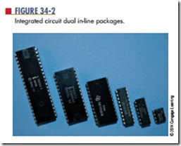
Integrated circuits are mounted in packages de- signed to protect them from moisture, dust, and other contaminants. The most popular package design is the dual in-line package (dIP) (Figure 34-2). DIPs are manufactured in several sizes to accommodate the

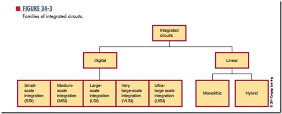
various sizes of integrated circuits: small-scale inte- gration (ssI) with up to 100 electrical components per chip (early 1960s), medium-scale integration (MsI) with 100 to 3000 electrical components per chip (late 1960s), large-scale integration (LsI) with 3000 to 100,000 electrical components per chip (mid-1970s), and very large-scale integration (VLsI) with 100,000 to 1,000,000 electrical components per chip (1980s). uLsI stands for ultra-large-scale integra- tion and provides no qualitative leap from VLSI but is reserved to emphasize chip complexity in marketing. Integrated circuit families are shown in Figure 34-3.
Wafer–scale integration (WSI), which uses uncut wafers containing entire computer systems including memory, was developed in the 1980s. It failed because of problems with creating a defect-free manufacturing process. WSI was followed by system-on-chip (SOC) design. This process takes components that were typically manufactured on separate chips and wired together on a printed circuit board and designs them to occupy a single chip that contains the whole electronic system: microprocessor, memory, peripheral interface, input/output logic control, a/d converters, and so on.
The pin count of the VLSI circuits in the 1980s exceeded the practical limits for DIP packaging. This led to pin grid array (Pga) and leadless chip carrier (Lcc) packages. Surface-mount packaging, which uses a fine lead pitch, became popular in the late 1980s. In the late 1990s, high pin count devices used plastic quad flat package (PQFP) and thin small outline package (tsoP) packaging.
The package is made in either ceramic or plastic. Plastic is less expensive and is suitable for most applications where the operating temperature falls between 32°F and 158°F (0°C and 70°C). Ceramic devices are more expensive but offer better protec- tion against moisture and contamination. They also operate in a wider range of temperatures of 267°F to 2193°F (255°C to 1125°C). Ceramic devices are recommended for military, aerospace, and severe industrial applications.
A small 8-pin DIP, called a mini-DIP, is used for de- vices with a minimum number of inputs and outputs. It is used mostly with monolithic integrated circuits.
A flat-pack is smaller and thinner than a DIP and is used where space is limited. It is made from metal or ceramic and operates in a temperature range of 267°F to 2193°F (255°C to 1125°C).
After the integrated circuit is packaged, it is tested over a wide range of temperatures to ensure that it meets all electrical specifications.
Questions
1. What are the functions of an integrated circuit package?
2. What package is most often used for integrated circuits?
3. What materials are used for integrated circuit packages?
4. What are the advantages of ceramic packages?
5. What is the advantage of the flat-pack inte- grated circuit package?