Integrated circuit construction techniques
Integrated circuits are classified according to their construction techniques. The more common construction techniques are monolithic, thin film, thick film, and hybrid.
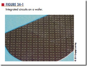
Monolithic integrated circuits are constructed in the same manner as transistors but include a few additional steps. The integrated circuit begins with a circular silicon wafer 3 to 4 inches in diameter and about 0.010 inch thick. This serves as a substrate (base) on which the integrated circuits are formed. Many integrated circuits are formed at the same time on this wafer—up to several hundred, depending on the size of the wafer. The integrated circuits on the wafer are generally all the same size and type and contain the same number and type of components (Figure 34-1).
After fabrication, the integrated circuits are tested on the wafer. After testing, the wafer is sliced into individual chips. Each chip represents one complete integrated circuit containing all the components and connections associated with that circuit. Each chip that passes quality control tests is then mounted into a package. Even though a large number of integrated circuits are fabricated at the same time, only a certain number are usable. This is referred to as the yield, which is the maximum number of usable integrated circuits compared with the rejects.
thin-film integrated circuits are formed on the surface of an insulating substrate of glass or ceramic, usually less than an inch square. The components (resistors and capacitors) are formed by an extremely thin film of metal and oxides deposited on the substrate. Thin strips of metal are then deposited to connect the components. Diodes and transistors are formed as separate semiconductor devices and attached in the proper location. Resistors are formed by depositing tantalum or nichrome on the surface of the substrate in a thin film 0.0001 inch thick. The value of the resis- tor is determined by the length, width, and thickness of each strip. Conductors are formed of low-resistance metal such as gold, platinum, or aluminum. This pro- cess can produce a resistor accurate to within + 0.1%. It can also obtain a ratio between resistors accurate to +0.01%. Accurate ratios are important for the proper operation of a particular circuit.
Thin-film capacitors consist of two thin layers of metal separated by an extremely thin dielectric. A metal layer is deposited on the substrate. An oxide coating is then formed over the metal for a dielectric. The dielectric is formed from an insulating material such as tantalum oxide, silicon oxide, or aluminum oxide. The top plate, formed from gold, tantalum, or platinum, is deposited on the dielectric. The capacitor value is obtained by adjusting the area of the plate and by varying the thickness and type of dielectric.
Diode and transistor chips are formed using the monolithic technique. The diode and transistor chips are permanently mounted on the substrate. They are then electrically connected to the thin-film circuit using extremely thin wires.
The materials used for components and conductors are deposited on the substrate using an evaporation or sputtering process. The evaporation process requires that the material deposited on the substrate be placed in a vacuum and heated until it evaporates. The vapors are then allowed to condense on the substrate, forming a thin film.
The sputtering process subjects a gas-filled chamber to a high voltage. The high voltage ionizes the gas, and the material to be deposited is bombarded with ions. This dislodges the atoms within the material, which drift toward the substrate, where they are deposited as a thin film. A mask is used to ensure proper location of the film deposit. Another method is to coat the substrate completely and cut or etch away the undesired portions.
In thick-film integrated circuits construction, the resistors, capacitors, and conductors are formed on the substrate using a screen-printing process: A fine wire screen is placed over the substrate, and metallized ink is forced through the screen with a squeegee. The screen acts as a mask. The substrate and ink are then heated to over 1112°F (600°C) to harden the ink.
Thick-film capacitors have low values (in picofarads). When a higher value is required, discrete capacitors are used. The thick-film components are 0.001 inch thick; they have no discernable thickness. The thick-film components resemble conventional discrete components.
hybrid integrated circuits are formed using monolithic, thin-film, thick-film, and discrete components. This allows for a high degree of circuit complexity by using monolithic circuits while taking advantage of extremely accurate component values and tolerances with the film techniques. Discrete components are used because they can handle relatively large amounts of power.
If only a few circuits are to be made, it is cheaper to use hybrid integrated circuits. The major expense in hybrid construction is the wiring and assembly of components and the final packaging of the device.
Because hybrid circuits use discrete components, they are larger and heavier than monolithic integrated cir- cuits. The use of discrete components tends to make hybrid circuits less reliable than monolithic circuits.
Questions
1. What methods are used to construct integrated circuits?
2. Describe the monolithic process of integrated circuit fabrication.
3. What are the differences between thin-film and thick-film fabrication processes?
4. How is a hybrid integrated circuit constructed?
5. What determines which process will be used when fabricating an integrated circuit?
Related posts:
Incoming search terms:
- integrated circuit construction techniques
- circuit construction methods
- technique used in fabrication of thin film and thick film ic
- monolithic thin film thick film and hybrid ICs construction techniques
- integrated circuit thin film technology English for IT
- IC CHIP Integrated Circuit Diode Transistor Capacitor mail
- construction techniques of a electric circuit
- construction of thin film ics
- construction of integrated cct
- construction of an integra
- constructing tecnique for ic
- construct monolithic ic for the circuit
- circuit construction with hef4077bp ic
- thin film and thick film technology in ic fabrication
