Signal Generators
Sinewave Oscillators
Variable frequency sinusoidal input test waveforms are used for determining the voltage gain, the system bandwidth, the internal phase shift or group delay, the maximum output signal swing, and the amount of waveform distortion introduced by the system under test. For audio purposes, a frequency range of 20 Hz to 20 kHz will normally be adequate, although practical instruments will usually cover a somewhat wider bandwidth than this. Except for harmonic distortion measurements, a high degree of waveform purity is probably unnecessary, and stability of output as a function “of time and frequency” is probably the most important characteristic for such equipment.
It is desirable to be able to measure the output signal swing and voltage gain of the equipment under specified load conditions. In, for example, an audio power amplifier, this would be done to determine the input drive requirements and output power that can be delivered by the amplifier. For precise measurements, a properly specified load system, a known frequency source, and an accurately calibrated RMS reading AC voltmeter would be necessary, together with an oscilloscope, to monitor the output waveform to ensure that the output waveform is not distorted by overloading.
Some knowledge of the phase errors (the relative time delay introduced at any one frequency in relation to another) can be essential for certain uses—for example, in long-distance cable transmission systems—but in normal audio usage such relative phase errors are not noticeable unless they are very large. This is because the ear is generally able to accept without difficulty the relative delays in the arrival times of sound pressure waves due to differing path lengths caused by reflections in the route from the speaker to the ear.
Oscillators designed for use with audio equipment will typically cover the frequency range 10 Hz to 100 kHz, with a maximum output voltage of, perhaps, 10 V rms. For general purpose use, harmonic distortion levels in the range of 0.5–0.05% will probably be adequate, although equipment intended for performance assessments on high-quality audio amplifiers will usually demand waveform purity (harmonic distortion) levels at 1 kHz in the range from 0.02% down to 0.005 %, or lower. In practice, with simpler instruments, the distortion levels will deteriorate somewhat at the high- and low- frequency ends of the output frequency band.
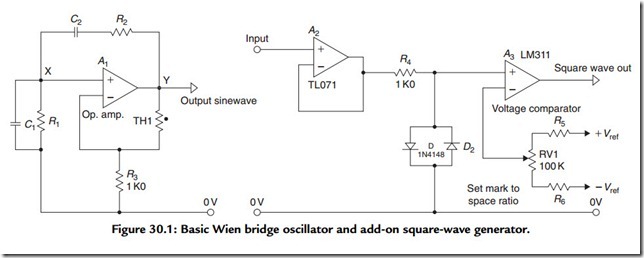
A variety of electronic circuit layouts have been proposed for use as sinewave signal generators, of which by far the most popular is the “Wien bridge” circuit shown in Figure 30.1. It is a requirement for continuous oscillation in any system that the feedback from output to input shall have zero (or some multiple of 360°) phase shift at a frequency where the feedback loop gain is very slightly greater than unity. Although to avoid waveform distortion, it is necessary that the gain should fall to unity at some value of output voltage within its linear voltage range.
In the Wien bridge, if R1 = R2 = R and C1 = C2 = C, the condition for zero phase shift in the network is met when the output frequency f0 = 1/(2πRC). At this frequency the attenuation of the RC network, from Y to X, in Figure 30.1, is 1/3. The circuit shown will therefore oscillate at f0 if the gain of the amplifier, Am, is initially slightly greater than three times. The required gain level can be obtained automatically by the use of a thermistor (TH1) in the negative feedback path and the correct choice of the value of R3.
Since C1R1 and C2R2 are the frequency-determining elements, the output frequency of the oscillator can be made variable by using a twin-gang variable resistor as R1/R2 or a twin gang capacitor as C1/C2. If a modern, very low distortion, operational amplifier, such as the LM833, the NE5534, or the OP27, is used as the amplifier gain block (A1) in this circuit, the principal source of distortion will be that caused by the action of the thermistor (TH1) used to stabilize the output signal voltage, where, at lower frequencies, the waveform peaks will tend to be flattened by its gain–reduction action. With an RS Components “RA53” type thermistor as TH1, the output voltage will be held at approximately 1 V rms, and the THD at 1 kHz will be typically of the order of 0.008%.
The output of almost any sinewave oscillator can be converted into square-wave form by the addition of an amplifier that is driven into clipping. This could be an opamp. A string of CMOS inverters, or, preferably, a fast voltage comparator IC, such as that also shown in Figure 30.1, where RV1 is used to set an equal mark to space ratio in the output waveform. An alternative approach used in some commercial instruments is simply to
use a high-speed analogue switch, operated by a control signal derived from a frequency stable oscillator, to feed one or an other of a pair of preset voltages, alternately, to a suitably fast output buffer stage.
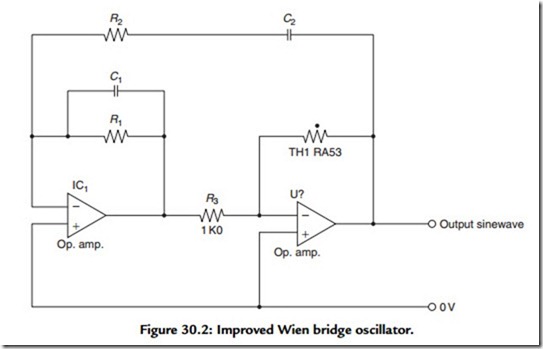
An improved Wien bridge oscillator circuit layout of my own, shown in Figure 30.2 (Wireless World, May 1981, pp. 51–53) in which the gain blocks A1 and A2 are connected as inverting amplifiers, thereby avoiding “common mode” distortion, is capable of a THD below 0.003% at 1 kHz with the thermistor-controlled amplitude stabilization layout shown in Figure 30.2, and about 0.001% when using the improved stabilization layout, using an LED and a photo-conductive cell, described in the article.
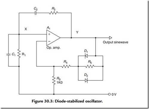
As a general rule the time required (and, since this relates to a number of waveform cycles, it will be frequency dependent) for an amplitude-stabilized oscillator of this kind to “settle” to a constant output voltage, following some disturbance (such as switching on, or alteration to its output frequency setting), will increase as the harmonic distortion level of the circuit is reduced. This characteristic is a nuisance for general purpose use where the THD level is relatively unimportant. In this case, an alternative output voltage
stabilizing circuit, such as the simple back-to-back connected silicon diode peak limiter circuit shown in Figure 30.3, would be preferable, despite its relatively modest (0.5% at 1 kHz) performance in respect of waveform distortion.
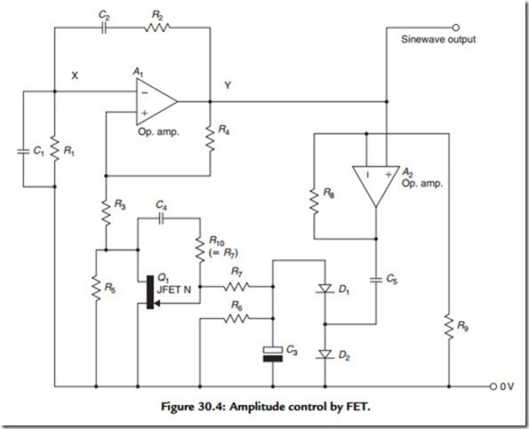
Rather greater control of the output signal amplitude can be obtained by more elaborate systems, such as the circuit shown in Figure 30.4. In this circuit, the output sinewave is fed to a high-input impedance rectifier system (A2/D1/D2), and the DC voltage generated by this is applied to the gate of an FET used as a voltage-controlled resistor. The values chosen for R6/R7 and C3/C4/C5 determine the stabilization time constant and the output signal amplitude is controlled by the ratio of R8:R9. In operation, the values of R4 and R3 are chosen so that the circuit will oscillate continuously with the FET (Q1) in zero-bias conducting mode. Then, as the –ve bias on the Q1 gate increases as a result of the rectifier action of Q1/Q2, the amplitude of oscillation will decrease until an equilibrium output voltage level is reached.
In commercial instruments, a high-quality small-power amplifier would normally be interposed between the output of the oscillator circuit and the output take-off point to
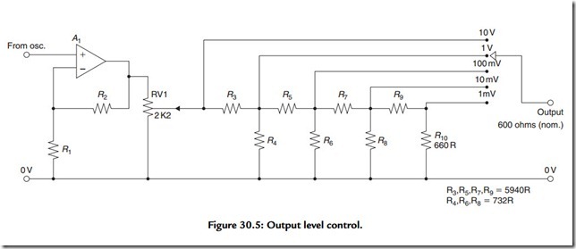
isolate the oscillator circuit from the load and to increase the output voltage level to, say, 10 V rms. An output attenuator of the kind shown in Figure 30.5 would then be added to allow a choice of maximum output voltage over the range 1 mV to 10 V rms, at a 600-Ω output impedance.
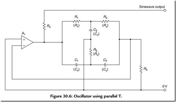
A somewhat improved performance in respect of THD is given by the “parallel T” oscillator arrangement shown in Figure 30.6, and a widely used and well-respected low- distortion oscillator was based on this type of frequency-determining arrangement. This differs in its method of operation from the typical Wien bridge system in that the network gives zero transmission from input to output at a frequency determined by the values of the resistors Rx, Ry, and Rz and the capacitors Cx, Cy, and Cz. If Cx = Cy = Cz/2 = C and
Rx = Ry = 2Rz = R, the frequency of oscillation will be 1/2πCR, as in the Wien bridge oscillator.
If the parallel T network is connected in the negative feedback path of a high gain amplifier (A1), oscillation will occur because there is an abrupt shift in the phase of the signal passing through the ‘T’ network at frequencies close to the null, and this, and the inevitable phase shift in the amplifier (A1), converts the nominally negative feedback signal derived from the output of the ‘T’ network into a positive feedback, oscillation-sustaining one.
A problem inherent in the parallel T design is that in order to alter the operating frequency it is necessary to make simultaneous adjustments to either three separate capacitors or three separate resistors. If fixed capacitor values are used, then one of these simultaneously variable resistors is required to have half the value of the other two. Alternatively, if fixed value resistors are used, then one of the three variable capacitors must have a value that is, over its whole adjustment range, twice that of the other two. This could be done by connecting two of the “gangs” in a four-gang capacitor in parallel, although, for normally available values of capacitance for each gang, the resistance values needed for the ‘T’ network will be in the megohm range. Also, it is necessary that the drive shafts of Cx and Cy be isolated from that of Cz.
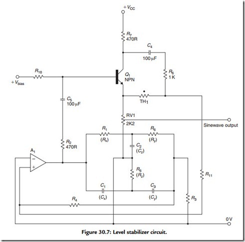
These difficulties are lessened if the oscillator is only required to operate at a range of fixed “spot” frequencies, and a further circuit of my own of this kind (Wireless World, July 1979, pp. 64–66) is shown in simplified form in Figure 30.7. The output voltage stabilization used in this circuit is based on a thermistor/resistor bridge connected across a transistor, Q1. The phase of the feedback signal derived from this, and fed to A1, changes
from +ve to –ve as the output voltage exceeds some predetermined output voltage level. The THD given by this oscillator approaches 0.0001% at 1 kHz, worsening to about 0.0003% at the extremes of its 100-Hz to 10-kHz operating frequency range.
It is expected in modem wide-range low-distortion test bench oscillators that they will offer a high degree of both frequency and amplitude stability. This is difficult to obtain using designs based on resistor/capacitor or inductor/capacitor frequency control systems, which has encouraged the development of designs based on digital waveform synthesis, and other forms of digital signal processing.
30.2.2 Digital Waveform Generation
Because of the need for a precise, stable, and reproducible output signal frequency in a test oscillator, a number of circuit arrangements have been designed in which use is made of the frequency drift-free output obtainable from a quartz crystal oscillator. Since this will normally provide only a single spot-frequency output, some arrangement is needed to derive a variable frequency signal from this fixed frequency reference source.
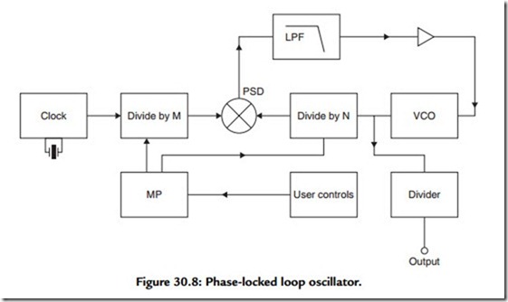
One common technique makes use of the “phase locked loop” (PLL) layout shown in Figure 30.8. In this, the outputs from a highly stable quartz crystal “clock” oscillator and from a variable-frequency “voltage-controlled oscillator” (VCO) are taken to a “phase- sensitive detector” (PSD)—a device whose output consists of the “sum” and “difference” frequencies of the two input signals. If the sum frequency is removed by filtration, and if the two input signals should happen to be at the same frequency, the difference frequency will be zero, and the PSD output voltage will be a DC potential whose sign is determined by the relative phase angle between the two input signals.
If this output voltage is amplified (having been filtered to remove the unwanted “sum” frequencies) and then fed as a DC control voltage to the VCO (a device whose output frequency is determined by the voltage applied to it), then, providing that the initial operating frequencies of the clock and the VCO are within the frequency “capture” range determined by the loop low-pass filter, the action of the circuit will be to force the VCO into frequency synchronism (but phase quadrature) with the clock signal: a condition usually called “lock.” Now if, as in Figure 30.8, the clock and VCO signals are passed through frequency divider stages, having values of ÷M and ÷N, respectively, when the loop is in lock the output frequency of the VCO will be Fout = Fck (N/M). If the clock frequency is sufficiently high, appropriate values of M and N can be found to allow the generation of virtually any desired VCO frequency. In an audio band oscillator, since the VCO will probably be a “varicap”-controlled LC oscillator, operating in the MHz range, the output signal will normally be obtained from a further variable ratio frequency divider, as shown in Figure 30.8. For the convenience of the user, once the required output frequency is keyed in, the actual division ratios required to generate the chosen output frequency will be determined by a microprocessor from ROM-based look-up tables, and the output signal frequency will be displayed as a numerical readout.
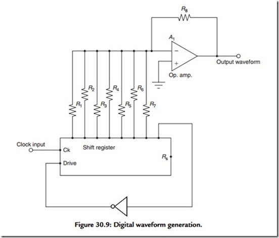
Given the availability of a stable, controllable frequency input signal, the generation of a low-distortion sinewave can, again, be done in many ways. For example, the circuit arrangement shown in Figure 30.9 is quoted by Horowitz and Hill (The Art of Electronics, 2nd ed. 667). In this, a logic voltage level step is clocked through a parallel output shift register connected to a group of resistors whose outputs are summed by an amplifier (A1). The output is a continuous waveform, of staircase type character, at a frequency of Fck/16.
If the values of the resistors R1–R7 are chosen correctly, the output will approximate to a sinewave, the lowest of whose harmonic distortion components is the 15th, at –24 dB. This distortion can be further reduced by low-pass filtering the output waveform. A more precise
waveform, having smaller, higher frequency staircase steps, could be obtained by connecting two or more such shift registers in series, with appropriate values of loading resistors.
Like all digitally synthesized systems, this circuit will have an output frequency stability that is as good as that of the clock oscillator, which will be crystal controlled. Also the output frequency can be displayed numerically and there will be no amplitude “bounce” on switch on, or on changing frequency.
A more elegant digitally synthesized sinewave generator is shown in Figure 30.10. In this the quantized values of a digitally encoded sine waveform are drawn from a data source, which could be a numerical algorithm, of the kind used, for example, in a “scientific” calculator, but, more conveniently, would be a ROM-based “look-up” table. These are
then clocked through a shift register into a 16-bit digital-to-analogue converter (DAC). If data chosen are those for a 16-bit encoded sinusoidal waveform, the typical intrinsic purity of the output signal will be of the order of 0.0007%, improved by the use of low- pass, sample-and-hold filtering.
Moreover, if digital filtering is used, prior to the DAC, this can be made to track the frequency of the output signal. As in the previous design (Figure 30.9) the output signal frequency is related to, and controlled by, the clock frequency.
