Electronic Circuits: Linear/Analog
The Building Blocks of Electronic Equipment
In this Chapter:
● Linear circuits defined.
● Types of linear circuits.
Characteristics and specifications of the most common linear circuits.
INTRODUCTION
The basic building blocks of electronic equipment are individual circuits made up of transistors, resistors, capacitors, and sometimes transformers, inductors or other components. It used to be that circuits were made up of individual discrete components that were wired together on a printed circuit board. But today, most electronic circuits are in integrated circuit (IC) form or more likely multiple circuits are already combined on a single silicon chip to create a larger circuit, sub-system or system on a chip (SoC).
While most circuits are ICs there are still some cases where discrete compo- nents are necessary or desirable. The most common examples are high voltage or high power circuits that would burn up a tiny silicon chip. Discrete compo- nents have not gone away entirely and you will find some of them external to an IC such as larger capacitors or inductors that just cannot be easily integrated on- to a chip or transistors that can handle higher voltage or power. As mentioned before, we are not going to talk about the make-up or operation of individual cir- cuits, Instead, this book treats circuits as just building blocks with an input and an output that process the input in some way to create a new, different output.
LINEAR CIRCUITS
There are two basic types of circuits, linear and digital. Digital circuits are cov- ered in the next chapter. Linear circuits are those circuits that process analog signals. Recall that analog signals are those that vary smoothly and continuously
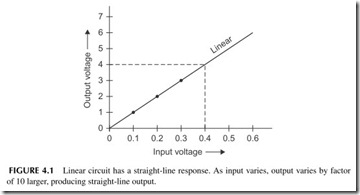
over time in contrast to pulse and digital signals that are voltages that switch off and on very fast. Analog signals are like sine waves, voice signals, video sig- nals, radio waves, and voltages from sensors like a temperature transducer. DC, either a constant value of voltage or one that is varying, is also an analog signal. A linear circuit is one whose output is proportional to its input. See Figure 4.1.
Its so-called response is a straight line or what a mathematician would call a linear function. The best example of this is the amplifier where its output is proportional to its input so that it accurately reproduces the input faithfully but at a higher voltage or power level. In the figure, with 0.4 volt input you get 4 volt output. That means the amplifier has a gain of 10. Linear circuits do not distort the signal. This chapter covers linear circuits with most of the emphasis on amplifiers since that is the largest category of linear circuits. And as it turns out, most other types of linear circuits are just amplifiers connected in different ways to give different processing results.
Amplifiers
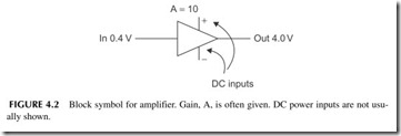
The basic block diagram symbol for an amplifier is a triangle. See Figure 4.2. It has an input and an output. Amplifiers also have one or more DC inputs as well. This DC from a battery or other power supply is what powers the circuit
and it is this DC that is ultimately converted into the new, larger output signal. In most cases the DC inputs are not shown in a block diagram. The ampli- fier processes the input to create an output of the same shape but at a larger amplitude.
The primary characteristic of any amplifier is its gain. The gain (usually represented by A) is simply a number equal to the ratio of the output to the input.
If the output is 4 volts and the input is 0.4 volt, the gain is simply:
The amplifier multiplies the input by 10 to get the output.
Output = 10 X Input
Classifying Amplifiers
The amplifier is the most common linear circuit. There are so many different types of amplifiers that we divide them up into different types to distinguish one from another. And there are multiple ways of doing this. Here are the most common.
Small Signal versus Large Signal
Small signal amplifiers are those that, as the name implies, only amplify small signals which are those roughly below about 1 volt. Small signal amplifiers amplify millivolt, microvolt, or nanovolt signals. Large signal amplifiers amplify larger signals and typically amplify the power of a signal rather than the voltage. These are called power amplifiers (PAs).
Frequency Classification
Amplifiers are also categorized by the frequency of the signals they amplify. Some examples are DC amplifiers, audio frequency (AF) amplifiers, interme- diate frequency (IF) amplifiers, video amplifiers, radio frequency (RF) ampli- fiers, and microwave amplifiers.
Configuration Classification
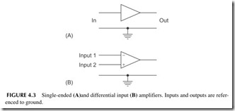
The two main configurations are single-ended and differential. A single-ended amplifier is one in which the input and output are referenced to a common ground. These amplifiers have two inputs, one is the signal and the other is ground. See Figure 4.3A. Normally only the input is shown as the ground is just assumed to be there.
A differential amplifier has two inputs as Figure 4.3B shows. These are usually called the inverting (-) and the non-inverting (+) inputs. Both inputs are referenced to ground. The amplifier is called a differential amplifier because it actually takes the mathematical difference between the two inputs and amplifies the result. One input is subtracted from another, then the differ- ence is amplified by the gain A. The formula for this operation is:
Output = (Input 2 – Input 1) X A
Differential amplifiers have one neat feature in that any signal common to both inputs like noise is automatically canceled out. This feature is widely taken advantage of in very small signal amplifiers used in memory chips and high gain amplifiers that amplify small signals from sensors. Noise that is picked up simultaneously on both inputs simply subtracts itself out without bothering the desired small difference signal.
Classification by Class of Operation
One way to categorize amplifiers is to designate the conduction of the tran- sistors in the amplifiers. The primary classes are A, B, AB, C, D, E, and F. There are a few others but these are the most common. Class A amplifiers conduct continuously. We say that the amplification occurs over the full 360 degrees of a sine wave cycle. See Figure 4.4. Note: The small t on the wave- forms means time as the voltage is varying over time.
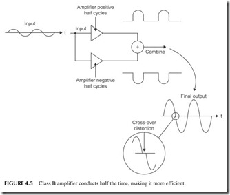
Class B amplifier transistors only conduct for half a cycle or 180 degrees of a sine wave. See Figure 4.5. Such an amplifier seems useless since it distorts the signal. But if you combine two transistors, one to amplify positive cycles and the other to amplify negative cycles, then combine the two, the complete wave is amplified. Such an amplifier is called a push pull amplifier. The ben- efit of this arrangement is that the circuit is more efficient.
Class AB amplifiers are a variation of the class B. Class B amps do add a little distortion to the signal around the point where the sine wave crosses zero. This is caused by the transistors not turning on and off precisely at the zero point. This glitch shown in Figure 4.5 is called crossover distortion. To get rid of that, class AB amplifiers allow some small current to flow continuously. The result is less distortion but a little less efficiency.
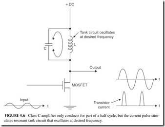
Class C amplifiers are for RF signals and are usually power amplifi- ers. They only allow the transistor to conduct for less than 180 degrees of a sine wave input, usually 90 to 150 degrees. It produces massive distortion. However, the amplifier output is made up of an inductor and capacitor (LC) tuned circuit that oscillates at the operating frequency and removes the distor- tion. These amplifiers are very efficient.
In a class C amplifier the MOSFET acts like a switch that is turned off and on by the input signal, usually a sine wave. See Figure 4.6. When the MOSFET is on the capacitor charges up to the DC supply voltage and current flows in the inductor creating a surrounding magnetic field. When the transistor turns off, the inductor and capacitor begin to exchange energy and set up an oscillation at the resonant frequency of the LC circuit. This is called a tank circuit. The result is that the energy stored in the tank circuit produces the amplified sine wave output.
Another way of looking at this is that the transistor switch distorts the input creating a pulse waveform that contains lots of harmonics. The tank circuit acts like a selective band-pass filter that lets the fundamental sine wave pass while the harmonics are filtered out.
Don ’t forget the Fourier theory and harmonics. Remember that a harmonic is an integer multiple of a fundamental sine wave. If the fundamental sine wave is 20 MHz, the 2nd harmonic is 40 MHz, the 3rd harmonic is 60 MHz, the 4th har- monic is 80 MHz, and so on. Any non-sine wave signal, like a half sine wave, square wave, or pulse is said to be made up of the fundamental sine wave added to multiple harmonics. A distorted sine wave has the fundamental sine wave in it but also har- monics. This concept is called the Fourier theory after the French mathematician.
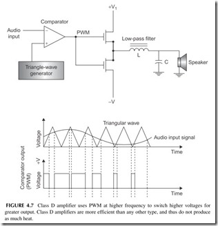
Class D amplifiers are a special class called a switching amplifier. It is made up of transistor switches rather than a real linear amplifier. This ampli- fier chops the input analog signal into high-frequency pulses with a varying width. See Figure 4.7. This process is called pulse width modulation (PWM).
The sine wave audio signal to be amplified is sent to one input of a special amplifier called a comparator along with a higher-frequency triangle wave. The comparator output switches when the triangle wave and sine wave values are equal. The resulting PWM signal is then fed to MOSFET switches to make the signal bigger. The higher amplitude output it then filtered back into an ana- log signal by a low-pass filter made up of a capacitor and inductor. Most class D amplifiers are audio power amplifiers whose load is a speaker or headphone. For low power less than a few watts, all the circuitry is in a single IC. For higher power, the MOSFETs are larger external devices.
The big benefit of switching amplifiers is that for a given output power they are very efficient. Whereas a class AB amplifier may only be 20 to 30% efficient, the class D is over 90% efficient. This means that the amplifier can be smaller and use less power and dissipates less heat. Class D amplifiers are great for portable battery-operated devices like MP3 players and cell phones.
Classes E and F are special switching amplifier variations used at RF fre- quencies only. Like the class C amplifier, they use LC circuits to filter out the harmonics they produce. They are very efficient.
Operational Amplifiers
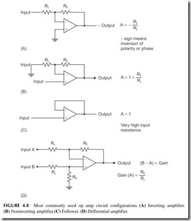
There are many special types of amplifiers. The most widely used is the opera- tional amplifier or op amp. This is a versatile high-gain DC differential ampli- fier that can be configured with external resistors, capacitors, diodes, etc. to perform a wide variety of amplification functions. The op amp may be the most widely used type of amplifier because of its versatility.
Figure 4.8 shows the most common op amp configurations. In most cases, the resistors are external to the IC amplifier. Note that the gain is determined by the values of the external resistors. Note formulas for gain (A).
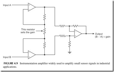
A variation of the op amp is the instrumentation amp. See Figure 4.9. It is a combination of multiple op amps that make it very useful in industrial applica- tions such as amplifying small signals from sensors. Again the gain is deter- mined by the resistor values. You can make this amplifier from individual op amps but usually you just buy it as a single integrated circuit. The external resistor sets the gain.
A variable or programmable gain amplifier is one whose gain can be con- trolled from an external DC input.
Amplifier Specifications
While you really do not need to know much about what the circuitry in an amplifier IC is, you do need to understand the specifications. Here are the most common specifications to look for.
As mentioned before, gain is the primary amplifier characteristic. It is usu- ally a voltage or power ratio, depending on the type of amplifier.
Voltage gain is output voltage over input voltage: ![]()
Power gain is output power over input power:![]()
Many amplifiers have their gain expressed in decibels (dB). A dB is a gain measurement based on a logarithmic scale rather than a linear scale. This has the advantage of being able to express large and small gains in smaller numbers.
And gains of multiple stages can be added rather than multiplied. To calculate dB gains you used these formulas:
Voltage gain: dB = 20 log (Av) Power gain: dB = 10 log (Ap)
In these formulas, log means the common (base 10) logarithm of the voltage or power gain. The logarithm (log) is easy to find using a scientific calculator.
For example, a voltage gain of 50 expressed in dB is:
dB = 20 log 50 = 20 (1.7) = 34 dB
A power gain 300 expressed in dB is:
dB = 10 log 300 = 10(2.5) = 25 dB
Input Impedance
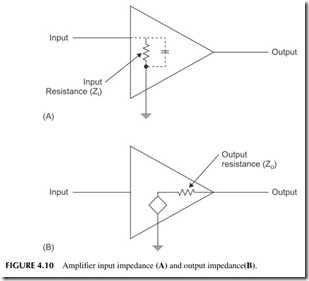
Input impedance is the load seen by the signal source to the amplifier. It is usu- ally resistive but typically also has some capacitance across it. Figure 4.10A shows an equivalent circuit of an amplifier. Note the input resistance. That is the input impedance. It may be as high as several megohms or could be as low
as, say, 50 ohms. Usually the higher the better for voltage amplifiers but not for power amplifiers.
Impedance
The term impedance means opposition to current flow. It is actually the combined opposition offered by resistance plus any capacitive or inductive reactance. If there is no reactance, the impedance is just the resistance so the two terms can be used interchangeably. Impedance is represented by the letter Z.
Output Impedance
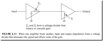
Amplifiers act as signal generating sources because they essentially just create a new higher voltage or higher power signal with the same shape as the input. They appear as a signal generator to the next circuit or load. Figure 4.10B shows the amplifier as a generator shaped as a diamond. It has an internal impedance or series resistance called the output impedance. It is not a real resistor but it is there and it appears in series with whatever load is connected which may be another amplifier or something else.
Figure 4.11 shows the amplifier connected to another amplifier. Note that the output impedance for amplifier A2 and the load form a voltage divider so some of the amplification is lost to the voltage divider effect. The input imped- ance of A2 is the load for the output impedance of A1.
Cascading Amplifiers
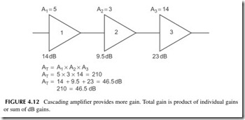
If an amplifier does not have enough gain, then multiple amplifiers can be cas- caded one after the other to give the needed gain. One amplifier amplifies the output of the next and so on. See Figure 4.12. To calculate the overall gain of an amplifier you just multiply the gains as shown in the figure. This procedure assumes that one amplifier does not load the next. That is, the output imped- ance of each amplifier is assumed to be zero and the input impedance of the next amplifier is assumed to be infinite. That way, there is no voltage divider effect that lowers the gain.
If the amplifier gains are given in dB, you just add the dB figures to get the total gain.
Efficiency
Efficiency is the ratio of the output power to the input power expressed as a percentage.
An amplifier takes the DC supply voltage and converts it into the AC out- put. The efficiency expresses how well the amplifier does this. Any lost power usually gets converted to heat which is not good. Nevertheless, some heat will always be generated just because electronic circuits are not perfect. High effi- ciency is a good thing of course, but often efficiency is traded off for better linearity, fidelity, and lower distortion of the signal.
Class A amplifiers have the poorest efficiency commonly in the 10 to 30% range. Classes B and AB are more efficient in the range of 50 to 70%. Class C amps have an efficiency of 70 to 85%. Class D amplifiers are the best with efficiencies in the 80 to 95% range.
Frequency Response
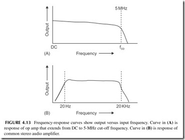
This is a measure of the range of frequencies that amplifiers cover. DC amplifiers may only cover DC up to about a few hundred Hz. Audio amplifiers may cover voice frequencies from 300 to 3000 Hz or stereo amps that cover 20 Hz to 20 kHz. IF amplifiers may only cover a specific band, say, 455 kHz, 9 MHz, 45 MHz, 70 MHz, or some other popular IF value. Op amps amplify signals from DC up to some very high frequency as high as several hundred MHz in some cases.
RF amplifiers cover high radio frequencies from a few MHz up to micro- waves from 1 to 100 GHz. Their frequency and range of coverage is usually set by a filter or LC tuned circuit.
Figure 4.13A shows the response curve for an op amp with an output down to DC and up to the cut-off frequency (fco) or 5 MHz. Figure 4.13B is the response curve of a stereo amplifier with a range of 20 Hz to 20 kHz.
Output Capability
This specification indicates the range of output signals the amplifier is capa- ble of. It is usually stated as a maximum voltage swing or as a maximum amount of output power. In both cases, the maximum output is usually given for a given value of load resistance. For example, an op amp may be capable of producing an output of ±12 volts across a 2 K load. A power amplifier may produce a maximum output of 10 watts across an 8 ohm speaker load or, say, 50 watts across a 50 ohm antenna load.
Filters
A filter is a frequency sensitive circuit that is designed to pass some frequen- cies, but reject others. There are various ways of making filter circuits that will accept some frequencies, but greatly attenuate others. There are literally thou- sands of applications for such circuits. But the main use of filters is to retain a desired signal, but eliminate interference and noise.
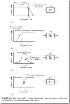
There are four basic types of filters: low-pass (LPF), high-pass (HPF), band- pass (BPF), and band-reject (BRF). The names, of course, tell their function.
A low-pass filter (LPF) is a circuit that passes all frequencies between DC and some upper cut-off frequency (fco ). All frequencies above the cut-off fre- quency are rejected. Figure 4.14A shows the response curve of an LPF. This is a plot of the filter output amplitude versus frequency. Note the gradual slope
as signals above the cut-off frequency (fc) are reduced in amplitude. The block symbol is how LPF is represented in some diagrams.
A high-pass filter passes frequencies above the cut-off and greatly attenu- ates those below the cut-off. Figure 4.14B shows the ideal response curve of an HPF. Note the HPF symbol.
Band-pass filters (BPF) pass a certain range of frequencies, but reject all those above and below that range. Figure 4.14C shows the practical response curve of a BPF. Note that there are two cut-off frequencies, one above and one below the center frequency fc . The difference between the upper and lower cut- offs is called the filter bandwidth (BW):
BW = f2 – f1
This is the range of frequencies passed. Again note the schematic symbol for a BPF.
Figure 4.14D illustrates the curve for a band-reject or notch filter. It is used to eliminate one single frequency and those close around it.
Note in the block symbols in Figure 4.14 that each has three waves repre- senting high, middle, and low frequencies. The wave with the slash through it means that these frequencies are cut out or greatly attenuated.
Filters can be implemented in many ways. Resistor and capacitor (RC) filters are common as are inductor and capacitor (LC) filters. You can make filters with op amps called active filters. Other filters are made with mechani- cal vibrating elements, a ceramic or quartz crystal, or a special surface acoustic wave (SAW) filter. Many filters today are made with digital signal processing (DSP). These will be discussed in Chapter 6.
Oscillators
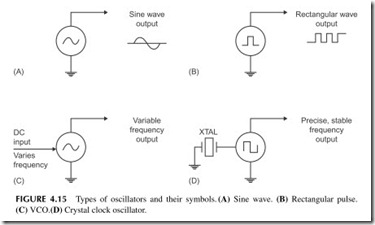
An oscillator is a circuit that generates a signal. It is usually a sine wave or a rectangular wave. The electronic symbols used to represent an oscillator are given in Figure 4.15.
The main specification of an oscillator is its output frequency. Most oscil- lators have a fixed frequency but there are oscillators whose frequency can be varied. A tunable frequency oscillator is called a variable frequency oscillator (VFO). You can often tune it by turning a knob that varies a capacitor or induc- tor to change the frequency. Some oscillators are tuned by an external voltage. These are called voltage-controlled oscillators (VCOs). By varying the value of a DC input voltage, the frequency is changed.
The frequency of an oscillator is set by some frequency determining ele- ment or circuit. That circuit may be made up of resistors and capacitors (RC), inductors and capacitors (LC), or a crystal. A crystal is a thin piece of quartz that can be made to vibrate at a very precise frequency. It maintains its fre- quency very closely unlike RC or LC networks that can drift with temperature or change from vibration or other conditions. Crystals come in a small metal package and are used to set the frequency in most oscillators today.
A special type of oscillator is called a clock oscillator. It is used as an accu- rate time and frequency source. The frequency determining element is usu- ally a quartz crystal that vibrates at a precise frequency and is very stable. The clock signal is used to operate all the circuits in synchronism. An example is the clock oscillator in a PC that sets the speed of calculations. Sometimes you will see a quartz crystal (XTAL) symbol drawn with the oscillator symbol to illustrate this. See Figure 4.14D.
Mixers
A mixer is a circuit that takes two input signals and mixes them in a special way to produce new output signals. There are two types of mixers, linear and non-linear.
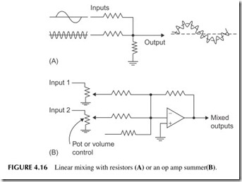
A linear mixer is one that takes the input signals and just adds them together. You can do this with some resistors as shown in Figure 4.16A. The sum of both input signals appears across the output resistor.
You can also make a linear mixer with an op amp as shown in Figure 4.16B. This op amp circuit is called a summer. Setting the resistor values allows you to mix and add gain at the same time. A good example of a linear mixer is those used by musicians so they can mix the outputs from microphones and musical instruments so they can all be amplified as one by the power amplifi- ers that drive the speakers. Note the variable resistors called pots that are used as amplitude or volume controls.
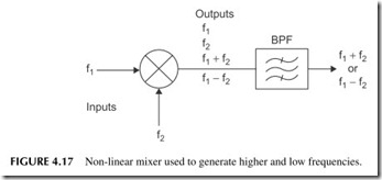
A non-linear mixer takes two input signals and effectively multiplies them together. The result is that the mixer produces four output signals. Figure 4.17 shows the symbol for a mixer. The inputs are frequencies 1 and 2 or f1 and f2.
The mixer outputs are f1, f2, and (f1 + f2 ) or the sum, and (f1 – f2 ) the differ- ence. The sum and difference frequencies are the ones of most interest. Usually a filter is used at the output of the mixer to select the desired frequency and eliminate the others. If the lower difference frequency is selected, the mixer is often called a down converter. If the sum frequency is selected, the mixer is called an up converter. The mixer is a way to translate a frequency to another higher or lower frequency that is better for processing. Any signal amplitude or frequency variations on the inputs are accurately carried through to the new output frequency.
Phase Detector
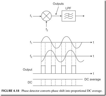
A phase detector is a mixer-like circuit that puts out a signal that is propor- tional to the phase difference between two input signals of the same frequency. See Figure 4.18. A phase shift is a time difference between two signals of the
same frequency. We sometimes need to know how much phase shift is present. The phase detector produces a series of output pulses whose width is pro- portional to the phase difference. Passing the pulses through a low-pass filter smoothes them into a proportional DC voltage.
Filtering Pulses into DC
A common occurrence in electronic circuits is the filtering of pulses into a DC voltage. You saw this back in Figure 3.15 where positive pulses from a sine wave rectifier are smoothed into a DC voltage. It is the capacitor that charges up and stores the pulse voltage. Then between pulses the capacitor discharges into the load maintaining a near constant DC voltage. The low-pass filter usually includes a capacitor so performs the same function in the phase detector of Figure 4.18. The output is a proportional average DC output.
Phase-Locked Loops
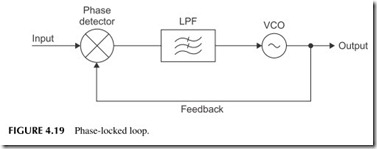
The phase-locked loop (PLL) is a frequency- and phase-sensitive feedback control circuit. It consists of three major parts: a mixer or phase detector, a low-pass filter (LPF), and a voltage-controlled oscillator (VCO), as shown in Figure 4.19. The signal from the VCO is compared to the input signal. If there is a frequency (or phase) difference between the two, an error signal is gener- ated. This error signal is filtered by the LPF into a varying DC level and is used to control the VCO frequency. This is the feedback signal.
If the VCO frequency, fo, differs from the input reference signal frequency, fo the fr the phase detector sees this as a phase shift. This causes the phase detector to produce an error signal. This error signal is filtered into a varying DC signal that is used to control the VCO.
The VCO can be either a sine wave oscillator or a rectangular wave oscil- lator depending upon the desired waveshape of the output. In either case, the VCO output frequency is made directly proportional to the DC control voltage. There is a linear voltage-to-frequency relationship in the VCO. This means that changing the control voltage produces a proportional change in output fre- quency. If the voltage goes up, so does the frequency.
Now if an input reference signal whose frequency is near that of the VCO is applied to the PLL, the phase detector will produce an output voltage pro- portional to the frequency difference. This signal is filtered and the resulting DC control voltage is applied to the VCO. The control voltage is such that it forces the VCO frequency to move in a direction that reduces the error signal. This means that the VCO frequency will change until it is equal to the input reference signal frequency. When this happens, the two signals are synchro- nized or “locked.” The phase difference causes the phase detector to produce the DC voltage at the VCO input to keep the PLL locked to the input signal.
If the input reference signal changes, then the phase detector will recognize a frequency (or phase) difference between the input and the VCO output. As a result, the LPF will produce a different DC control signal that will force the VCO to change such that it is equal to the new input frequency. As you can see then, the PLL will “track” an input signal frequency as it changes.
The range of frequencies over which the PLL will track an input signal and remain locked is known as the lock range. This is a range of frequencies above and below the VCO free running frequency. The PLL can track and “lock” to any input frequency in this range. If an input signal out of the lock range is applied, the PLL will not synchronize.
If the input signal is initially outside of the lock range, the PLL will not lock. But, the PLL will jump into a locked condition as soon as the input fre- quency gets close to the VCO frequency. In other words, the PLL will “capture” the incoming signal if it is close enough to the VCO frequency. Once the input
signal is captured, the PLL is locked and will track further changes in the input signal frequency.
The range of frequencies over which a PLL can capture a signal is known as the capture range. Like the lock range, it too is centered on the free running frequency. But the capture range is narrower than the lock range. The PLL acts as a frequency sensitive circuit over a narrow range of frequencies.
Since the PLL will only capture and lock on to input signals within a cer- tain narrow band, the PLL acts like a band-pass filter. For that reason, the PLL is an excellent signal conditioner. You can take a noisy input signal or one with undesirable interference on it and filter it with a PLL. The PLL will lock on to only the desired frequency component of the input. The VCO repro- duces the input signal at the same frequency but with the noise and interfer- ence removed. The PLL not only cleans up a signal but also can track it if its frequency changes.
The PLL is widely used for a variety of purposes. It is used to recover the clock signal in some wireless applications. It is used to recover the original signal in frequency modulation (FM) radio. It is used to multiply a frequency by a fixed factor. It can be used for motor speed control. Almost all electronic products of some kind contain a PLL.
Frequency Synthesizers
One of the most popular uses of the PLL is in frequency synthesizers. A fre- quency synthesizer is a very stable signal source that can be varied over a spe- cific range of frequencies in finite increments or steps. Frequency synthesizers are used as precision signal generators for test and measurement purposes and replace more conventional oscillator circuits as the primary signal sources in radio transmitters or receivers.
The big advantage of a PLL synthesizer is its ability to generate a wide range of frequencies with great accuracy and stability by using only a single stable signal source. For example, a PLL synthesizer with a single crystal con- trolled reference input can readily generate hundreds or even thousands of discrete frequencies that are as stable as the crystal reference. By using a syn- thesizer as the initial signal source in a transmitter, a wide range of channels can be obtained with a single crystal. When many channels must be used, a synthesizer greatly reduces the cost since crystals are expensive.
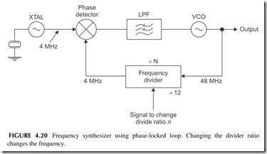
The synthesizer circuit in Figure 4.20 shows that it is a PLL with a fre- quency divider connected between the VCO output and the phase detector. The frequency divider is a circuit that divides its input frequency by some whole number. For example, the output of a divider with a division factor of 12 and an input of 48 MHz is 48/12 = 4 MHz.
The frequency synthesizer PLL also uses a stable, crystal oscillator input to the phase detector. This is usually derived from a crystal oscillator. When the PLL is locked, the stability and accuracy of the VCO output will be the same
as that of the reference input. The frequency divider is usually made so that its divide ratio can be changed by setting a switch or changing the control inputs. Changing the division ratio changes the output frequency at which the loop will lock.
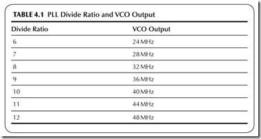
The reason for this is that the two inputs to the phase detector must always be equal in frequency if a locked condition is to be achieved. The reference frequency is fixed so the only thing that can change is the VCO output if the divider ratio is altered. If the loop is locked, the output of the divider will be 24 MHz no matter what the divide ratio is. Therefore, with an output of 4 MHz, a divide by 6 circuit must have a 24 MHz input. Since the VCO output is the divider input, the VCO and synthesizer output will be 24 MHz too.
As you can see, changing the divide ratio changes the output frequency. In this circuit, if the divide ratio is changed in integer values between 6 and 12, the output frequencies will be as shown in Table 4.1. With this setup, the out- put is switched in 4-MHz increments.
If the input reference is made 1 MHz, then when the divide ratio is changed, the output frequency will step in 1-MHz increments. By carefully selecting the reference frequency and the divide ratio, it is possible to synthesize practically any range of frequencies in many increments from subaudio to microwave.
Note one final fact about the PLL circuit in Figure 4.20. If the reference is considered the input, and the VCO is considered the output, then the PLL is acting as a frequency multiplier. Here the output is 12 times the input. You will occasionally see the PLL used as a frequency multiplier in some applications.
The PLL synthesizer is a very versatile circuit. It is commonly available in integrated circuit form. PLL frequency synthesizers are used in TV channel selectors, stereo receivers, CB radios, cellular telephones, and other two-way radios. In such equipment the divider ratio is supplied by an input keyboard or
a built-in microcomputer programmed to supply the desired divide factor for a selected output frequency.
Power Supplies
A power supply is, as its name implies, a source of power to an electronic cir- cuit. Most electronic circuits operate from DC as they process AC or DC sig- nals. The most common power supply is the one that gets its input from the standard AC wall outlet that supplies 120 volts at 60 Hz. This common voltage is then converted by the power supply into one or more DC voltages that go to operate the TV set, computer, or other equipment. This section discusses the main components and circuits of a power supply.
Batteries
One of the most widely used power supplies is a battery. A battery is a great source of DC by itself and no AC source is needed. Batteries were the very first form of voltage sources for electrical circuits and they are still widely used today. What would we do without the batteries for our cell phones, iPods, cordless telephones, laptop computers, and remote controls? Just remember that a special form of power supply is the battery charger that normally uses AC to recharge lead-acid, nickel cadmium, nickel metal hydride, and lithium- ion batteries.
Standard Power Supply
A very common AC to DC power supply is shown in Figure 4.21. It normally consists of a transformer that translates the 120 volt AC line voltage into a higher or lower voltage as needed by its step up or step down characteristics. Today, since most equipment uses ICs, a lower AC voltage is needed. The lower
AC voltage is then converted into a pulsating DC voltage by a rectifier. A rec- tifier is one or more diodes that act like polarity sensitive switches to change the positive and/or negative sine half cycles into pulses of DC. A filter is then used to smooth the pulses into a more constant DC voltage. The filter is usually a large capacitor that charges up to the peak of the DC pulses then only dis- charges very slowly into the load.
Regulators
A regulator is a circuit that maintains a fixed DC output voltage of a desired value. The DC produced by the power supply at the filter output will vary over a wide range as the AC input line voltage changes. Any changes in the load meaning variations in current taken from the supply will also cause the output voltage to vary. A regulator absorbs those variations and creates a constant DC output suitable for powering ICs and other electronic circuits. Common DC output voltages are 3.3, 5, 12, 15, and 24 volts. Other typical DC supply volt-ages are 1.2, 1.8, 6, and 48 volts.
There are two types of regulators, linear and switching. A linear regulator inserts a transistor in series between the power supply output and the load. If the load varies, circuitry in the regulator adjusts the conduction of the transis- tor so that a constant voltage is maintained. It is as if a resistor in series with the load forms an adjustable voltage divider. If the output voltage drops, the series transistor conducts more to keep the output voltage the same. If the out- put increases, the transistor conducts less to decrease the voltage and maintain the same value.
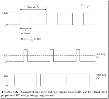
The other type of regulator is the switching regulator. It puts a transistor in series with the load as well but the internal circuitry turns the transistor off and on at a high rate of speed. By varying the duty cycle (ratio of on to time for one period) of the on–off pulses the average DC output may be varied. Then if any output voltage changes are sensed, the duty cycle is adjusted to ensure that the average output stays the same.
Duty Cycle and PWM
The duty cycle is the ratio of the pulse width to the period of a rectangular wave as shown in Figure 4.22 . The period is the reciprocal of the frequency of the signal or T = 1/f. It is constant. The on-time is the duration of the pulse voltage (t). The pulse duration can vary depending upon what the application is. If the period is 50 milliseconds and the pulse on-time is 10 milliseconds, the duty cycle (D.C.) is:
D.C. = 10/50 = 0.2 X 100 = 20%
Circuits can be made to change the on-time so that the duty cycle can be varied from a few percent to nearly 100%. This is called pulse width modula- tion (PWM). It was introduced earlier in the class D amplifier discussion. PWM is widely used in switching power supplies like regulators and DC–DC converters.
Keep in mind that if you filter the pulses into an average proportional DC with a capacitor or LPF, you can vary the DC from some low value with a low duty cycle or some higher value with a higher duty cycle.
Linear regulators work very well but are not very efficient as they waste power in the series transistor. Typical efficiency is 10 to 40%. A switching reg- ulator is far more efficient as it is off for a large part of the time. Efficiencies in the 70 to 95% range are common.
DC—DC Converters
A DC–DC converter is a circuit that does what its name implies. It translates one DC voltage to another. It can take the voltage from a 12 volt battery and generate several hundred or thousand volts. Or it can take a 4.2 volt battery and produce voltages of 3.3 or 2.5 volts and 15 volts. By building one DC power supply, several other output voltages can be obtained by using different DC–DC converters.
Bus-Oriented Architecture
Many power supplies have what we call a bus architecture. See Figure 4.21. The DC power supply produces one main output voltage. That voltage is applied to a common DC bus. A bus is just the name for the two + and – DC lines that carry the voltage. Then, regulators and DC–DC converters are used to generate the voltages needed by the equipment. Again see Figure 4.21.
Power Management
Many power supplies today include a circuit that manages the power supply voltages. It is usually a single IC that does things like turn on the various DC voltages in a power supply in a specific sequence. Some ICs require multiple DC voltages and they must be turned on one at a time in a specific sequence. In addition, the power management chip does things like monitor current usage. If one power supply is not being used, meaning current not being drawn from it, that part of the power supply is shut down to conserve power. A good exam- ple of this is the power management in a laptop computer or cell phone that monitors and controls all DC power to preserve the battery charge for longer life. Some other functions performed by power management chips are voltage monitoring with voltage alarm if a voltage fails, temperature monitoring, fault detection, over voltage or under voltage detection, and power control. Some power management chips also have the battery charging circuits built in. Every cell phone and laptop has one of these.
Inverters
An inverter is a power supply that converts DC into AC. A common unit con- verts 12 volts from a car battery into standard 120 volt 60 Hz AC. With an inverter you can operate common household lights and appliances from a battery.
A special variation of an inverter is the uninterruptible power supply (UPS). These are widely used with computers and networks to provide power even during loss of AC input from the power line. A battery operates an inverter that is used to power the computers and other equipment. If the AC power fails, the equipment continues to operate. The battery is continuously charged by a built-in battery charger that operates from the AC power line.
Solar Power System
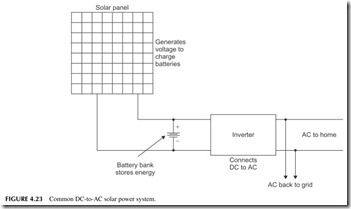
Any home or business solar power system is similar to a large UPS (see Figure 4.23). It uses the solar panels to charge a bank of batteries that store the energy for use later when the sun goes down. The inverters convert the DC into standard 120/240 volt AC to power the house. In some cases, unused power is sent back to the power grid.
Project 4.1
Build a Kit
If you are really serious about electronics, then one of the first things you should do is build a kit. A kit, in case you really do not know, is a complete package of electronic parts to make a specific product. You build it yourself by placing com- ponents on a printed circuit board (PCB) and soldering them in place. There is no better way to see how electronic products get put together than to handle the wide variety of parts. It is a great learning experience.
There are two main questions to answer about this project. First, what kind of kit do you want? Second, can you learn to solder? You will have to answer the first question, but as for the second, yes, you can learn to solder. It’s not that hard.
One way to get an overview of the kits available is to obtain catalogs from the sources mentioned earlier in this book. You can order a print copy online and see the whole range of kits available. Go to:
All Electronics: www.allelectronics.com Elenco Electronics: www.elenco.com Jameco: www.jameco.com
Kelvin: www.kelvin.com
Ramsey: www.ramseyelectronics.com
What I recommend is to get a kit related to one of the topics in this chapter. A power supply is a great choice, and it will give you a variable DC voltage source that you can use in future projects. The same is true for a basic audio amplifier. A solar panel kit is a good one also. Most of the companies have lots of radio- and wireless-related kits, but save these for the later chapters on wireless products.
Don’t forget to get a small soldering iron (25 watts or so) with a small tip and some solder. You will also need a few hand tools such as a wire stripper, needle- nose pliers, side cutters, and a small screwdriver, if you do not already own these.
