10.8 DEVELOPMEN T OF CIRCUIT 4
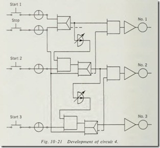
This circuit is to provide sequence speed control with definite time delay . The motor must be started in its first speed by START button 1 and can then be raised to its second speed by means of START button 2, after a time delay to allow for acceleration. The motor may then be raised to its third speed by START button 3, after a time delay. The STOP button stops the motor regardless of the speed at which it is running.
The logic statement for the first speed is: Run when the START button is closed and the STOP button is closed . A MEMORY will be needed because of the momentary contact of the START button.
The logic statement for the second speed is: Run when the START button is closed and the time delay has lapsed since the first speed was energized.
The logic statement for the third speed is: Run when the START button is closed and a time delay has lapsed since the second speed was energized. The completed circuit is shown
Fig. 20 ·21. The NOT outputs of the MEMORYs are used to shut down each lower speed when necessary.
10 · 9 DEVELOPMENT OF CIRCUIT 5
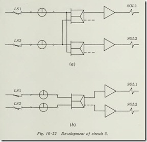
There are two solenoids on the machine. The first solenoid, SOL 1, is to turn on when momentary-contact limit switch LS1 is closed. The solenoid must remain on until shut off by the closing of momentary-contact limit switch LS2. The closing of LS2 must also turn on a second solenoid, SOL 2, which will remain on until shut off by the momentary closing of LSl on the next cycle of the machine.
Since the contacts of LSI and LS2 are closed only momentarily and the solenoid must remember whether they were turned off or turned on, the circuit will require the use of retentive MEMORY elements.
When LSl is connected to the ON input of one MEMORY unit and the OFF input of a second MEMORY unit (Fig. 10·22a), half of the requirements of the circuit will be satisfied.
When LS2 is connected to the OFF input of the first MEMORY and the ON input of the second MEMORY, the required circuit will be complete. This circuit can be simplified by utilizing the inverted, or NOT, output of only one MEMORY as shown in Fig. 10·22b.
10·10 OFTEN-USED RELAY EQUIVALENTS
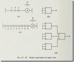
An y number of relay contacts connected in series (Fig. 10·23a) can be represented by equivalent AND circuitry (Fig. 10·23b ) . Sometimes it may be necessary to use more than one AND ele ment to provide the required number of inputs. Figure 10·23c and d illustrates how nine inputs can be provided when only three-inpu t AN D elements are available.
The logic equivalent of paralleled normally open relay contacts is the OR (Fig. 10 ·24).
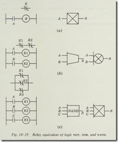
Relays with normally closed contacts become a NOT (Fig. 10·25a), a NOR (Fig. 10·25b), or a NAND (Fig. 10·25c), de pending upon the number of contacts and how they are connected.
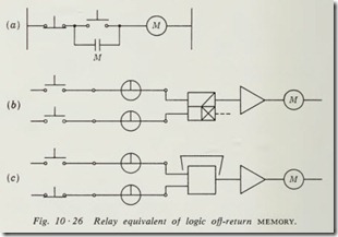
The popular off-return of the magnetic control using three wire control (Fig. 10·26a) can be duplicated in logic circuits by using an off-return MEMORY (Fig. 10·26b). The static circuit can also have the NOT, or inverted, output of the intended func tion shown by dotted lines on the symbol or by a NOT symbol within the MEMORY symbol. The circuit of Fig. 10·26c provides the same basic control using a sealed (feedback) AND and allows
other inputs to be used.
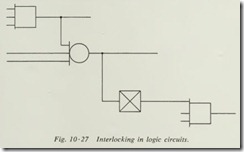
Interlocking, which is so important in machine and process control, is easily achieved in logic circuitry by using the output of a logic function in one part of the circuit as one of the inputs to another logic element in a different part of the circuit (Fig. 10·27).
10·11 THE TRANSISTOR AS A STATIC SWITCH
The logic diagram gives complete information on the operation of the control system but tells nothing about the circuit of the
logic element itself. When a system is installed it must use the logic elements made by only one manufacturer, because two systems are not generally compatible. The voltage and current requirements for the logic elements differ between manufacturers.
Once a particular manufacturer’s system is chosen, the instal ler can be confident that the individual logic elements will work when properly connected in accordance with the logic diagram. Power supplies are designed to supply all the correct voltages. Signal converters are designed to supply the correct input for the logic elements. The output of each logic element is designed to provide the proper input for other logic elements or amplifiers. Since the interconnection requirements are built into the logic elements, it is not absolutely necessary for the installer or service man to fully understand the actual circuit of the logic element itself. General practice is to replace a defective element or return it to the factory if repair is to be attempted. The installer or serviceman will need specific installation information on the indi vidual system he is working with, and will be much better prepared to clear or prevent trouble if he understands how the logic
elements work.
All commercially available logic components use the transistor as the basic switching device. During the late 1950s, logic ele ments were designed around a saturable reactor; however, these are no longer manufactured except for replacement in existing systems.
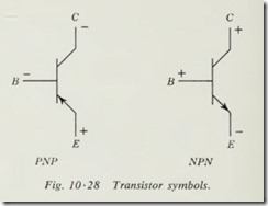
To understand transistorized logic components, you must first understand how a transistor responds to voltage and current. Figure 10·28 shows the symbols for NPN and PNP transistors with the necessary polarity for full conduction. The three exter nal leads are identified by their correct names: C for collector,B for base, and E for emitter. Conventional current flow is al ways used in transistor circuits and is indicated by arrows on the symbols.
The transistor is a semiconductor device which has two circuits: emitter to base and emitter to collector. The emitter-to base circuit is generally referred to as the base circuit. The emit ter-to-collector circuit is referred to as the power or output circuit.
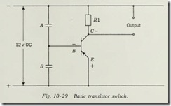
Consider the circuit of Fig. 10·29. When contact B is closed,the base of the transistor is at the same potential as the emitter,
and the transistor will not conduct from emitter to collector. For general circuit analysis, consider the emitter-to-collector cir cuit to be an open switch whenever the base of a PNP transistor is at zero voltage difference from the emitter. The same result will be achieved whenever the base is more positive than the emitter.
Whenever the base of a PNP transistor is made sufficiently more negative than the emitter, the transistor will conduct emit ter to collector . The emitter-to-collector circuit acts as a closed switch, wit h practically no voltage drop across the transistor. When contact A (Fig. 10·29) is closed and contact B is open, the base is at -12 volts. The transistor will conduct from emitter to base and, by transistor action, will also conduct from emitter to collector. The current is determined by the resistance of R . If the output voltage is taken from the output lead to the negative bus, the output voltage will be 12 volts. This is, of course, due to the voltage drop across R, which must equal the line voltage.
The previous explanation should make the switching action clear. When the base of the transistor (Fig. 10·29) is positive, with contact B closed and contact A open, the output is at zero volts because there is no voltage drop across R. When the base is negative, with contact A closed and contact B open, the output is at 12 volts because of the voltage drop across R .
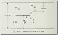
Because of various design considerations, it is desirable that the switch be conducting when no signal is applied and stop conducting when a signal is applied. In a slight modification of the circuit (Fig. 10·30), contact A is replaced by resistor R2, and resistor R4 is added. Resistors R2 and R4 form a volt age divider across the line voltage. Proper selection of R2 and R4 will provide the ideal value of negative potential at the base in order to provide full conduction in the emitter-to-collector circuit. The transistor is now conducting and has an output voltage of 12 volts. The closing of contact B will connect the base lead to the positive line and cause the transistor to cut off , thus reducing the output to zero volts. Consider contact B to be the pilot device used to control the switch. When the contact is closed, there is an input to the switch, but there is no output. When the contact is not closed, there is no input to the switch, but it does have an output. This action is known as a NOT or in verted logic. This is the building block upon which all tran sistorized logic elements are built. Different manufacturers will use different circuit arrangements to achieve the NOT operation of the transistor. However, the analysis given above will suffice to explain the operation of the transistor switch itself.
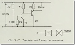
When the NOT action of the transistor switch (inverted logic) is not desirable, a second transistor is added to the basic circuit.
Figure 10·31 shows the new circuit. When contact B is closed, T1 will not conduct. The base of T2 is then at a negative value in relation to its emitter, because of the circuit from emitter to base through R 1 to the negative line. The negative potential on the base of T2 will cause it to conduct, producing a current through R3 and an output of 12 volts.
When contact B is open, T1 conducts and brings the base of T2 to the same potential as the positive bus; therefore T2 is cut off, and there is no output. The transistor switch is now a combi nation of two NOT basic circuits and produces an output when there is an input. When there is no input, there is no output.
10 ·12 THE TRANSISTOR SWITCH AS AN AND ELEMENT
The basic transistor switch can be made to perform the AND function by proper input circuitry. The actual circuits will be considered in later chapters, but a symbolic representation here should improve the student’s understanding.
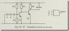
Figure 10·32 shows the basic switch connected through con tacts A, B, and C in series. The switch cannot have an output
until the base of Tl is connected to the positive bus and cuts off Tl.Resistance voltage dividers are generally used for a prac tical input circuit. The circuit is arranged so that proper input voltage must be applied to all inputs before the base voltage will become sufficiently positive to cut off Tl.
If the second transistor, T2, had been left off of the basic transistor switch, the result would have been an AND-NOT element.
10· 13 THE TRANSISTOR SWITCH AS AN OR ELEMENT
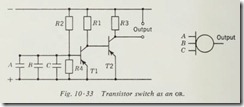
Figure 10 ·33 shows the basic transistor switch connected to three contacts in parallel. If any one of these contacts, A or B or C, were closed, the base of T1 would be connected to the posi tive line and T 1 would be cut off.
The actual input circuit for the transistor switch is made up of resistors and/ or diodes. When they are properly connected, the OR input circuit must make the base of T1 positive when any one or a combination of its inputs has the proper input voltage applied.
If the second transistor T2 had not been used in the transistor switch circuit, the result would have been an OR-NOT or NOR element.
Chapters 11 to 13 will take up the actual commercial circuits in detail. Each manufacturing concern has its own design to accomplish what the symbolic circuits in this chapter illustrate.
Summary
Static control systems are built by properly interconnecting five basic building blocks: AND, OR, NOT, MEMORY, and time DELAY.
The information section of the control circuit usually consists of conventional contact-type sensing devices. Signals of relatively high voltage from the information section of the system are modified by signal converters to the proper low-voltage direct current required by the logic elements of the decision section. The action section of the system converts the low-voltage, low power signal from the decision section into the power required by the device to be controlled.
All available logic elements are built around the basic transis
tor switch but differ in the application of specific circuitry.
Development of static control circuits has been approached as an extension of electromagnetic control development as cov ered in Chap. 6. The principles are rather simple but require practice. The serious student should practice developing many circuits to perfect his approach. When it is possible to actually wire the circuits after development, a higher degree of proficiency should result.
The five steps in logic circuit development are:
1. Convert the specifications into English logic statements.
2. Draw each statement in logic-symbol form.
3. Integrate and interconnect the individual statements.
4. Combine functions where possible to simplify the circuit.
5. Review the overall circuit and check it against the specifications.
Review Questions
1. What are the requirements of an AND element?
2. What are the requirements of an OR element?
3. What are the requirements of a NOT element? What are the requirements of a NOR element?
4. Describe the action of the off-return MEMORY element when the power fails and returns.
5. Describe the action of the retentive MEMORY element when the power fails and returns.
6. Draw the proper symbol for each of the following: AND, OR, NOT, NOR, NAND, retentive MEMORY, Off-return MEMORY, and the four types of time DELAY.
7. Develop a logic circuit that will energize a solenoid when a normally open momentary-contact START button is pressed. The solenoid must remain on until a second nor mally open momentary-contact STOP button is pressed.
8. Develop a logic circuit for the following specifications. A coil must be energized when normally open limit switch LSI is closed and pressure switch PSI is closed and thermo stat Tl is closed or when normally open push button PBl is closed and thermostat T2 is closed.
9. Develop a logic circuit for the following specifications. A signal light is to turn on whenever normally open contacts A, B, C, and D are all closed, provided normally closed contacts E and F are not open.
10. What is the function of the signal converter?
11. What is the function of the output amplifier?
