RECORDER/AMPLIFIER CIRCUITS
A 4W tape recorder amplifier and a tape preamplifier are described, and the modifications necessary for stereo operation are considered. An automatic gain control circuit for use with tape recorders is also included.
A 6W universal amplifier is described. It incorporates an equalising preamplifier, an active tone control circuit and a BEL IC-CA810 in the power output stage. The performance characteristics of the amplifier are also given.
4 W TAPE RECORDER
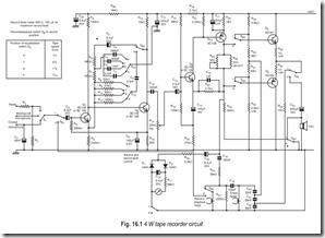
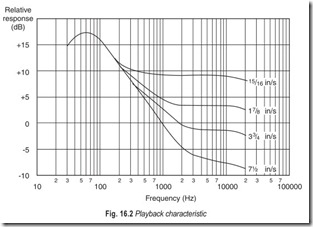
The 4W tape recorder, shown in Fig 16.1, uses silicon transistors in the first three stages to obtain high sensitivity. The output stage uses a complementary matched pair, transistor AD 161npn and AD 162 pnp which are also used for the oscillator during recording. Equalisation is provided for tape speeds of 7 1/2 ips (19.1 cm/s), 3 3/4 ips (9.5 cm/s), 17/8 ips (4.75 cm/s), and 15/16 ips (2.4 cm/s), which conforms to CCIR Standards where appropriate.Playback: The BC 109 has been chosen for the input stage because it is particularly suitable for use in audio input stages where low noise is essential. Its collector is directly connected to the base of Q2 ; its emitter is connected via an RC network to the collector of Q . This RC network provides a path for negative feedback by means of which equalisation is effected. The frequency response curves on playback are shown in Fig. 15.2.
A dc feedback path is also provided from the emitter of Q2 to the base of Q1 . The dc feedback along thispath stabilises the working points of Q1 and Q2 .
The other transistors in the tape recorder form a conventional amplifier. The complementary pair of Q5 and Q6 is driven by Q4, which is itself driven by the high-gain BC 148 or BC 108 transistor. Potentiometer R23 is adjusted to given a quiescent output stage current of 5 mA.
Record: Different input circuits are needed to match the different signal sources. For example, the input circuit for a crystal microphone contains a shunt capacitor. C1, and that for a radio receiver is a potential divider. A moving coil-microphone, however, can be connected directly because the amplifier has an input resistance of 200 kW. During recording, Q5 and Q6 operate as an oscillator at 50 kHz, the erase head being used as an oscillator coil. The capacitive taps, C20, C21, and C22 also provide the necessary conditions for sustained oscillation.The recording level indicator gives a reading proportional to the peak-to-peak voltage at the collector of Q4 . The full recording level with a sine wave is 4V rms, which produces a current of 95 µA through the meter and 110 µA rms through the recording head.
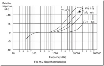
During recording, the equalisation circuits connected to switch SC are not used; feedback is via the path C3 , R6 and R7 , which has been designed to give treble boost. The frequency response curves on record are shown in Fig. 16.3.
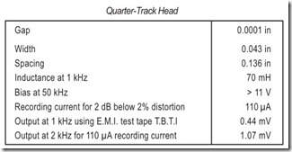
The recording current is taken from the collector of Q . Record/Playback heads with a larger inductance are not suitable because they would require larger bias voltage. The recording head has the following characteristics :
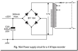
Power Supply : The circuit for a simple power supply suitable for use with the above tape recorder is shown in Fig. 16.4. It contains a main transformer with a secondry output of 17 V. This is rectified by means of bridge rectifier type BY 164, and smoothed by means of a 640 µF capacitor.
Performance :
Overall frequency response
Tape speed = 7 ½ ips 55 Hz to 20 kHz
Tape speed = 3 ¾ ips 55 Hz to 12 kHz
Tape speed = 1 7/8 ips 55 Hz to 6 kHz
Playback
Output power 4 W rms
Sensitivity at base of Q1 , at 1 kHz and with tape speed of 7 ½ ips 400 µV
Distortion for 4 W output 1.2%
Noise relative to 4 W, with volume control set so that a signal produced with 110 µA recording current gives 4 W output;
3 dB band width = 30 Hz to 15 kHz
Tape speed = 7 ½ ips – 60 dB
Tape speed = 3 ¾ ips – 57 dB
Tape speed = 17/8 ips – 55 dB
Tape speed = 15/16 ips – 50 dB
Record
Sensitivity at base of Q1 , for 110 µA recording 110 µV
current, with volume control at maximum setting
Distortion at full record level 1%
Recording current level for 4 W output, with volume 40 µA
control at maximum setting
TAPE PREAMPLIFIER
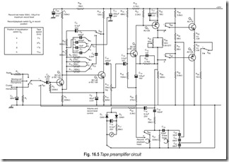
Circuit Description: Fig. 16.5 shows a preamplifier circuit derived from the tape recorder circuitry already described. The oscillator stage in this circuit uses a complementary pair comprising one AC 176 and one AC 128 transistor.
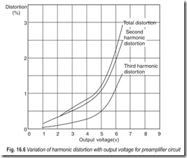
Performance: The distortion measured at the collector Q4 of transistor (AC 128) in the playback position is shown in Fig. 16.6. The measurements were made at a speed of 3 3 4 ips, although these characteristics vary little with speed. At a speed of 7 1/2 ips with the volume control at maximum , the output voltage is 6.55 V for an input voltage of 400 µV. The total current drain on playback is 25 mA.
MODIFICATIONS FOR STEREO OPERATION
In a stereo recording system,the bias and erase frequencies of the two channels must be equal, if the production of audio beat frequencies is to be prevented. Therefore, the bias and erase power for the two channels must be derived from one common oscillator or from two oscillators which have their frequencies locked together. The arrangement shown is Fig. 16.5 can be used for the preamplifier of Fig. 16.1 only if the AC 176/AC128 pair is replaced by an AD 161/AD 162 pair and the emitter resistors reduced accordingly.
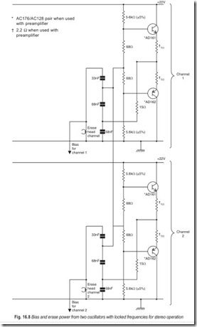
In the alternate arrangement in Fig. 16.8 two AC 176/AC 128 pairs will operate satisfactorily.
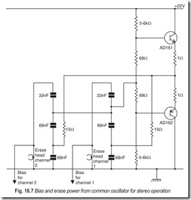
Bias and erase power from a common oscillator : A circuit that uses a common oscillator for stereo operation is given in Fig. 16.7. This shows that the two tuned erase heads, which form the load and feedback circuits of one of the complementary pairs of transistors, are in parallel. The bias for the two recording heads however, is still derived from the erase voltages across the erase heads as in the mono design. This has the advantage that the other pair of complementary transistors used for the output stage during playback may now be used as a monitoring facility.
Bias and erase power from two oscillators with locked frequencies : A circuit that uses two locked identical oscillators for stereo operation is given in Fig. 16.8. Locking of the oscillators is achieved by connecting together the two feedback paths.
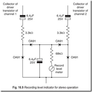
Recording level indicator : Fig 16.9 shows a recording level indicator for stereo operation. The meter gives a reading proportional to the peak-to-peak voltage at the collector of the driver transistor in the channel which has the highest recording level. For an input of 4 V rms (this corresponds to the rms voltage at the collector of the driver transistor when distortion due to tape saturation becomes significant) the d.c. current through the meter is 95 µA.
AGC CIRCUIT FOR TAPE RECORDERS
When recording on tape, the current in the recording head must not exceed the value at which tape saturation occurs if severe distortion is to be avoided. This can be prevented by monitoring the current by means of a meter or l.e.d. and manually adjusting the recording level. Another method is to use a circuit that electronically reduces the gain of the amplifier when the optimum recording level is exceeded.
To ensure that the distortion is recorded for only a short time, the gain control must respond very rapidly to the overload signal. When the gain has been reduced, however, the recovery time must be long, for otherwise volume compression will result, and loud and soft passage of music will be recorded with equal loudness.
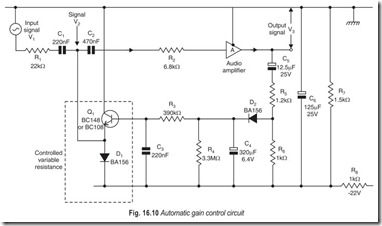
A gain control circuit that uses a minimum of components and can produce an attenuation of 40 dB within 150 milliseconds is shown in Fig. 16.10. The recovery rate does not exceed 6 dB per minute. With a faster recovery rate, the same circuit arrangement is suitable as a volume compressor in other applications.
Circuit Description : Gain control is achieved by means of an attenuator containing a diode.Controlling the direct current through the diode controls its slope resistance and consequently, the amount of attenuation.
The severe harmonic distortion caused by the exponential characteristic of one diode can be reduced by using two diodes in a reverse-parallel arrangement. In the circuit in Fig. 16.10 the base-emitter junction of a transistor is used as one of the diodes. Because the transistor is needed as a dc amplifier, this arrangement saves the expense of one diode.
Part of the amplifier output is rectified and used to provide the gain control signal. The time constants of the rectifier circuit are such as to give the high rate of attenuation and the long recovery time.
In Fig. 16.10, unit A is the audio amplifier and R2 represents its input resistance, which should be about 7 kΩ.
The variable attenuator comprises R1, C1, D1 and part of transistor Q1. Because C3 is a short circuit to ac signals, the base-emitter junction of the transistor is, in effect, in reverse-parallel with D1 for all ac signals.Resistors R5 and R6 form a fixed attenuator by means of which a constant fraction of the output is fedback to the control circuit. The feedback voltage is rectified by D2 , charges C4 , and is applied through R3 to the base of Q1 Hence, the voltage across C4 controls the current through Q1 3and D1 .With an input signal well below that which causes tape saturation, the voltage across C4 is low. Therefore the transistor current is also low and the slope resistance of the transistor and diode are high. Consequently, the shunting effect on the input to the amplifier is negligible.As the input signal is increased the voltage across C4 and the current through Q1 will also increase.
Eventually, the transistor current will reach a value which produces a significant reduction in the slope resistance of D1 . The voltage drop across R1 will be increased and there will be an appreciable attenuation of the signal to the amplifier. This occurs when the amplifier has an output of approximately 2 V rms.
A further increase in the input produces another rise in the voltage across C4. The consequent increase in transistor current now produces a rapid reduction in the diode slope resistance. The shunting effect of the transistor and diode on the input to the amplifier is greatly increased, and V2 is much less than V1.Once attenuation has started, voltages V2 and V3 remain practically constant. Over the full range of attenuation, 40 dB, they increase slightly because of slight increases in VBE , the forward voltage of D1 , at higher currents (of the order of 300 µA), and the base current through R3 .The attack time is determined by the time constant of C4 and the source impedance of the chargingcircuit, which is R5 in parallel with R6 . For an attack time of about 200 ms, the source impedance should be 600 W.The recovery time is determined by the time constant of C4 and its discharge circuit — R4 in parallelwith R3 and the slope resistance of Q1 and D1 . Over a wide range of attenuation, R3 is much larger than theslope resistances of the transistor and the diode. The rate of discharge of C4 is then controlled by the valueof R3 , and consequently, the rate of change of attenuation is constant. At very low transistor currents, the slope resistances of the transistor and the diode greatly exceed R3 , and the rate of discharge of C4 via the transistor is very low. This tends to make the rate of change of attenuation also very low. Under theseconditions, however, R4 provides an alternative discharge path. Hence, the rate of change of attenuation has a low limit that is determined by the value of R4 . When R3 is large with respect to the slope resistances of thetransistor and the diode, the effect of R4 is negligible.
The transistor is a BC 148 or BC 108 npn planar type, which, with its low leakage current and high gain, makes this simple arrangement possible. The silicon diodes also are used because of their low leakage currents.
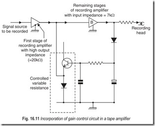
In Fig. 16.10 the gain is controlled by attenuating the signal before it reaches the audio amplifier. This has the disadvantage that, when the signal is attenuated, the noise originating in the first transistor of the amplifier is unaffected. A better arrangement would be to have the attenuation after the first stage of the amplifier thus reducing noise and signal simultaneously. The arrangement is shown in Fig. 16.11. A high voltage is required to operate the attenuating circuit; this will probably be available only at the output of the stage feeding the recording head.
Use of Electrolytic Capacitors in Timing Circuits : The maximum leakage currents quoted in published data on electrolytic capacitors are too high for use in long time constant circuits. Experience suggests, that the leakage currents of capacitors taken off the shelf will be low enough or will soon fall to a suitably low value. Therefore, electrolytic capacitors of a suitable type are readily available. At the worst, a tape recorder which has been stored for a very long time will have an initial recovery time slightly shorter than normal, but this will rapidly approach the normal value.
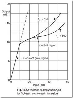
Performance : When the circuit controls the gain, the signal V2 is not maintained exactly constant nor completely independent of the amount of attenuation. This is shown in Fig. 16.12 by the input/output characteristics of the circuit with high-gain and low-gain transistors. When a low-gain transistor is used an attenuation of 40 dB is accompanied by an increase of 7 dB in the output, with a high-gain transistor, the corresponding increase in output is 4–5 dB.
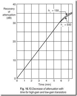
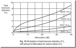
The change of attenuation with time is shown in Fig. 16.13. This diagram shows that the rate of change of attenuation is substantially constant over much of the range. It does not exceed 6 dB per minute and is almost independent of the gain of the transistor.The variation of total harmonic distortion (T.H.D.) of V2 with the amount of attenuation for variousvalues of V2 is given in Fig. 16.14. These curves show that V2 should not exceed 4 mV rms. if the T.H.D. isnot to exceed 2%.
6 W UNIVERSAL HI-FI AMPLIFIER
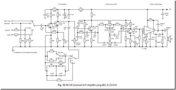
The circuit diagram of a 6 W Universal hi-fi amplifier is shown in Fig. 16.15. The salient features of this circuit are :
1. Inputs for magnetic and ceramic pick-ups, tape playback heads and radio receivers.
2. Active tone control network, providing more than 20 dB dynamic range for both bass and treble.
3. Very low distortion.
The amplifier consists of an equalising preamplifier, an active tone control circuit and a CA 810 power output stage. To achieve better noise figures for the amplifier stage, the preamplifier uses a low-noise npn transistor BCM 149 (Q1 ) at its input. The noise from the power supply is minimised by the decoupling network R1 – C1 and R2 – C2 .
The output of this low-noise transistor is direct coupled to another npn transistor BC 148 (Q2 ). The base bias for the input transistor Q1 is derived from the emitter of Q2 to achieve better dcstability. The required equalisation characteristic for different inputs is realised by appropriate feedback rom collector of Q2 to the emitter of the input transistor Q1 .
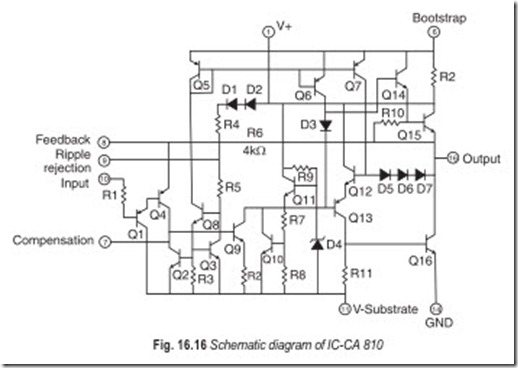
The output of the preamplifier is connected to the tone control circuit through a buffer transistor Q3 . The active tone control circuit uses an amplifier, Q4 , and a frequency dependent network to obtain the required tone control characteristics. The power output stage makes use of IC-CA 810 and delivers 6 W power into an 8 W load. Typical performance characteristics of this amplifier are given below.
Performance Characteristics
1. Supply voltage 18 V
2. Minimum output power 6 W
3.Input sensitivity for P0 = 50 mW
Radio 4 mV/100 kΩ
Ceramic pick-up 15.8 mV/1 MΩ
Magnetic pick-up 0.7 mV/50 kΩ
Tape input 0.8 mV/ 20 kΩ
4. Input sensitivity for maximum power output
Radio 35 mV
Ceramic pick-up 185 mV
Magnetic pick-up 6.1 mV
Tape input 8.8 mV
5. Zero signal current 12 mA
6. Supply current at maximum output power 430 mA
