U and D MOSFETs
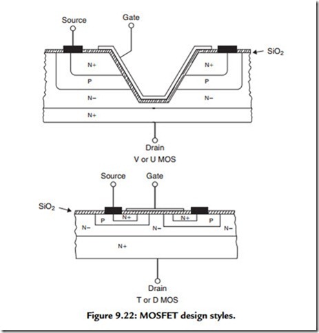
I have, so far, lumped all power MOSFETs together in considering their performance. However, there are, in practice, two different and distinct categories of these, based on their constructional form, and these are illustrated in Figure 9.22. In the V or U MOS devices—these are just different names for what is essentially the same system, depending on the profile of the etched slot—the current flow, when the gate layer has been made sufficiently positive (in the case of an N-channel device) to induce a mobile electron layer, will be essentially vertical in direction, whereas in D-MOS or T-MOS construction the current flow is T shaped from the source metallization pads across the exposed face of the very lightly doped P region to the vertical N-/N+ drain sink. Because it is easier to manufacture a very thin diffused layer (=short channel) in the vertical sense than to control the lateral diffusion width, in the case of a T-MOS device, by surface masking, the U-MOS devices are usually much faster in response than the T-MOS versions, but the T-MOS equivalents are more rugged and more readily available in complementary (N-channel/P-channel) forms.
All power MOSFETs have a high input capacitance, typically in the range of 500–2500 pF, and because devices with a lower conducting resistance (Rds/on) will have achieved this quality because of the connection of a large number of channels in parallel,
each of which will contribute its own element of capacitance, it is understandable that these low channel resistance types will have a larger input capacitance. Also, in general, P-channel devices will have a somewhat larger input capacitance than an N-channel one. The drain/gate capacitance—a factor that is very important if the MOSFET is used as a voltage amplifier—is usually in the range of 50–250 pF. The turn-on and turn-off times are about the same (in the range 30–100 nS) for both N-channel and P-channel types, mainly determined by the ease of applying or removing a charge from the gate electrode. If gate-stopper resistors are used—helpful in avoiding UHF parasitic oscillation and avoiding latch-up in audio amplifier output source followers—these will form a simple low-pass filter in conjunction with the device input capacitance and will slow down the operation of the MOSFET.
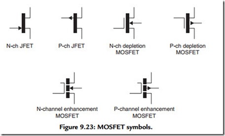
Although circuit designers tend to be rather lazy about using the proper symbols for the components in the designs they have drawn, enhancement-mode and depletion-mode MOSFETs should be differentiated in their symbol layout, as shown in Figure 9.23. As a personal idiosyncrasy, I also prefer to invert the symbol for P-channel field effect devices, as shown, to make this polarity distinction more obvious.

