Emitter–Follower Systems
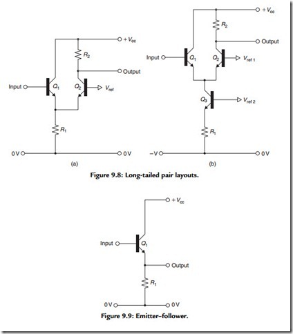
These are the solid-state equivalent of the valve cathode follower layout, although offering superior performance and greater versatility. In the simple circuit shown in Figure 9.9 (the case shown is for an NPN transistor, but a virtually identical circuit, but with negative supply rails, could be made with a similar PNP transistor), the emitter will
sit at a quiescent potential about 0.6 V more negative than that of the base, and this will follow, quite accurately, any signal voltage excursions applied to the base. (There are some caveats in respect of capacitative loads; these potential problems will be explored under the heading of slew rate limiting.) The output impedance of this circuit is low because this is approximately equal to 1/gm, and the gm of a typical small-signal, silicon BJT is of the order of 35 mA/V (35 mS) per mA of emitter current. So, if Q1 is operated at 5 mA, the expected output impedance, at low frequencies, will be 1/(5.35) kilohms, or 5.7 ohms, a value that is sufficiently smaller than any likely value for R1, that the presence of this resistor will not greatly affect the output impedance of the circuit.
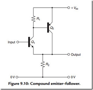
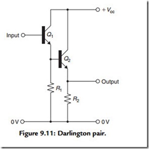
The output impedance of a simple emitter–follower can be reduced still further by the circuit elaboration shown in Figure 9.10, known as a compound emitter–follower. In this, the output impedance is lowered in proportion to the effective current gain of Q2 in that, by analogy with the output impedance of an operational amplifier with overall NFB, any change in the potential of the Q1 emitter, brought about by an externally impressed voltage, will result in an opposing change in the collector current of Q2. This layout gives a comparable result to that of the Darlington pair, of two transistors, in cascade, connected as emitter–followers, shown in Figure 9.11, except that the arrangement of Figure 9.10 will only have an input/output DC offset equivalent to a single emitter-base
forward voltage drop, whereas the layout of Figure 9.11 will have two, giving a combined quiescent voltage offset of the order of 1.3–1.5 V. Nevertheless, in commercial terms, the popularity of power transistors, connected internally as a Darlington pair, mainly for use in the output stages of audio amplifiers, is great enough for a range of single chip Darlington devices to be offered by the semiconductor manufacturers.


