Control of Operating Bias
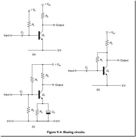
There are three basic ways of providing a DC quiescent voltage bias to a BJT, which is shown in Figure 9.4. In the first of these methods, shown in Figure 9.4(a), an arrangement that is fortunately seldom used, the method adopted is simply to connect an input resistor, R1, between the base of the transistor and some suitable voltage source. This voltage can then be adjusted so that the collector current of the transistor is of the right order to place the collector potential near its desired operating voltage. The snag with this scheme is that transistors vary quite a lot from one to another of nominally the same type, so this would require to be set anew for each individual device. Also, if the operating temperature changes, the current gain of the device (which is temperature sensitive) will be altered and, with it, the collector current of Q1 and its working potential. The arrangement shown in Figure 9.4(b) is somewhat preferable in that a high current gain transistor, or one working at a higher temperature, will pass more current, and this will lower the collector voltage of Q1, which will, in turn, reduce the bias current flowing through R1. However, this also provides NFB and will limit the stage gain to a value somewhat less than R1/Zin.
The method almost invariably used in competently designed circuitry is that shown in Figure 9.4(c), or some equivalent layout. In this, a potential divider (R1,R2) having an output impedance low in relation to the base impedance of Q1 is used to provide a fixed DC base potential. Since the emitter will, by emitter–follower action, sit at a potential, depending on emitter current, which is about 0.6 V below that of the base, the value of R4 will then determine the emitter and collector currents, and the operating conditions so provided will hold good for almost any broadly similar device used in this position.
Since the emitter resistor would cause a significant reduction in stage gain, as seen in the equivalent analysis of valve cathode bias systems, it is customary to bypass this resistor with a capacitor, C2, which is chosen to have an impedance low in relation to R4 and R3.
