Circuit Oddments
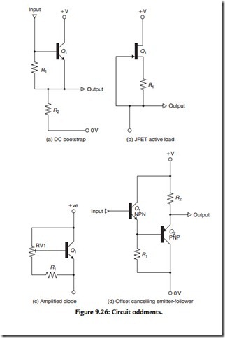
Several circuit modules have found their way into amplifier circuit design, and some of the more common of these are shown in Figure 9.26. Both the DC bootstrap, shown
in Figure 9.26(a), and the JFET active load, shown in Figure 9.26(b), act to increase the dynamic impedance of R1, although the DC bootstrap, which can, of course, be constructed using complementary devices, has the advantage of offering a low output impedance. The amplified diode, shown as Figure 9.26(c), is a device that is much used as a means of generating the forward bias required for the transistors used in a push– pull pair of output emitter followers, particularly if it is arranged so that Q1 can sense the junction temperature of the output transistors. It can also be used, over a range of relatively low voltages, as an adjustable voltage source to complement the fixed voltage references provided by zener and avalanche diodes, band-gap references (IC stabilizers designed to provide extremely stable low voltage sources), and the wide range of voltage stabilizer ICs. Finally, when some form of impedance transformation is required, without the Vbe offset of an emitter follower, this can be contrived as shown by putting two complementary emitter followers in series. This layout will also provide a measure of temperature compensation.
