Useful Circuit Components
By comparison with the situation that existed at the time when most of the pioneering work was done on valve-operated audio amplifiers, the design of solid-state amplifier systems has been facilitated greatly by the existence of a number of circuit artifices, contrived with solid-state components, which perform useful functions in the design. This section shows a selection of the more common ones.
Constant Current Sources
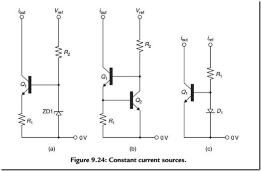
A simple two-terminal constant current (CC) source is shown in Figure 9.17, and devices of this kind are made as single ICs with specified output currents. By comparison with the discrete JFET/resistor version, the IC will usually have a higher dynamic impedance and a rather higher maximum working voltage. In power amplifier circuits it is more common to use discrete component CC sources based on BJTs, as these are generally less expensive than JFETs and provide higher working voltages. The most obvious of these
layouts is that shown in Figure 9.24(a), in which the transistor, Q1, is fed with a fixed base voltage—in this case derived from a zener or avalanche diode, although any suitable voltage source will serve—and the current through Q1 is constrained by the value chosen for R1 in that if it grows too large, the base-emitter voltage of Q1 will diminish and Q1 output current will fall. Designers seeking economy of components will frequently operate several current source transistors and their associated emitter resistors (as Q1/R1) from the same reference voltage source.
In the somewhat preferable layout shown in Figure 9.24(b), a second transistor, Q2, is used to monitor the voltage developed across R1 due to the current through Q1; when this exceeds the base emitter turn-on potential (about 0.6 V), Q2 will conduct and will steal the base current to Q1 provided from Vref through R2. In the very simple layout shown in Figure 9.24(c), advantage is taken of the fact that the forward potential of a P-N junction diode, for any given junction temperature, will depend on the current flow through it. This means that if the base-emitter area and doping characteristics of Q1 are the same as those for the P-N junction in D1 (which would, obviously, be easy to arrange in the manufacture of ICs), then the current (iout) through Q1 will be caused to mimic that flowing through R1,
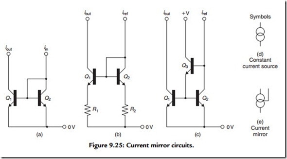
which is labeled iref. This particular action is called a current mirror, and several further versions of these are shown in Figure 9.25.
Current Mirror Layouts
Current mirror (CM) layouts allow, for example, the output currents from a long-tailed pair to be combined, which increases the gain from this circuit. In the version shown in Figure 9.25(a), two matched transistors are connected with their bases in parallel so that the current flow through Q2 will generate a base-emitter voltage drop that will be precisely that which is needed to cause Q1 to pass the same current. If any doubt exists about the similarity of the characteristics of the two transistors, as might reasonably be the case for randomly chosen devices, the equality of the two currents can be assisted by the inclusion of equal value emitter resistors (R1,R2) as shown in Figure 9.25(b). For the perfectionist, an improved three-transistor current mirror layout is shown in Figure 9.25(c). Commonly used circuit symbols for these devices are shown in Figures 9.25(d) and 9.25(e).

