Voltage-Clamping Devices
Voltage-clamping components are not subject to the power-follow problems common in crowbar systems. Clamping devices include selenium cells, zener diodes, and varistors of various types. Zener diodes, using improved silicon rectifier technology, provide an effective voltage clamp for the protection of sensitive electronic circuitry from transient disturbances. On the other hand, power dissipation for zener units is usually somewhat limited, compared with other suppression methods.
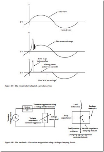
Selenium cells and varistors, although entirely different in construction, act similarly on a circuit exposed to a transient overvoltage. Figure 15.5 illustrates the variable nonlinear impedance exhibited by a voltage-clamping device. The figure also shows how these components can reduce transient overvoltages in a given circuit. The voltage-divider network established by the source impedance Zs and the clamping- device impedance Zc attenuates voltage excursions at the load. It should be understood that the transient suppressor depends upon the source impedance to aid the clamping effect. A protection device cannot be fully effective in a circuit that exhibits a low source impedance because the voltage-divider ratio is reduced proportionately. It also must be recognized that voltage-clamp components divert surge
currents; they do not absorb them. Care must be taken to ensure that the diversion path does not create new problems for the ac power system.
A typical voltage-vs.-current curve for a voltage-clamping device is shown in Figure 15.6. When the device is exposed to a high-voltage transient, the impedance of the component changes from a high standby value to a low conductive value, clamping the voltage at a specified level. The clamping effect common with this class of devices is illustrated in Figure 15.7.
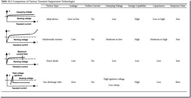
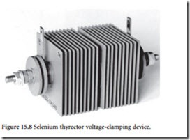
A selenium thyrector device, intended for low- to medium-power applications, is shown in Figure Voltage-clamping components are available in a variety of configurations, from high-power chassis- mount units to surface-mount devices designed for use on printed wiring boards. Selenium-cell transient suppressors can handle high-energy transients and repeated hits very well, but have poor voltage-clamping ability. Combination units are available, however, that use selenium devices, custom-fabricated to minimize the undesirable characteristics and to take advantage of the desirable ones. Table 15.1 compares the attributes of a variety of transient-suppression technologies.
At the clamping voltage, the clamping-device impedance goes low, but it does not fall to nearly zero, as occurs with crowbar devices [3]. There is, therefore, essentially no short-circuit magnitude follow cur- rent. Clamping voltage is maintained on the system load. The lower the source impedance, however, the more difficult it is for the clamping device to maintain system voltage without drawing excessive current.
Clamping devices operate in the nanosecond range, thousands of times faster than crowbar devices, but are generally capable of dissipating considerably less transient energy. They effectively clamp voltage spikes to a maximum level but have no effect on notches or brief dropouts.
High Low Slow
Metal-oxide varistors (MOVs), the most common of the clamping devices, are available for use at a wide range of voltages and cur- rents. The range of parameters includes:
• Voltages as low as 4 V for data lines up to several thousand volts for power sys- tems
• Peak pulse currents from a few amperes up to tens of thousands of amperes
• Energy dissipation from less than 1 to over 10,000 joules
MOVs are low in cost, compact in size, and easy to apply, and are among the most frequently used devices for transient protec-
tion. One disadvantage of the MOV is that its operating characteristics deteriorate with repeated transients. Although this problem has been reduced with improved technologies, MOV life under frequent transient conditions must be considered.
Silicon-carbide varistors have high power-handling capability and are used in high-voltage surge (lightning) arresters. The devices tend to draw considerable current in the normal state, and so they are commonly used in series with a gap that provides an open circuit until a surge occurs. This property makes silicon-carbide varistors unsatisfactory for low-voltage clamping operation. Newer zinc-oxide lightning arresters have better nonlinear characteristics and can be used without a gap. They are essentially crowbar devices, but perform almost like clamping devices.
Zener Components
Zener diodes exhibit high impedance below the zener or avalanche voltage (VZ), and very low impedance above VZ. Because of these clipping characteristics, the zener diode is often used to suppress transients [4]. Zeners are intolerant of excessive stress, and so it is important to know the power-handling capability for short pulse durations.
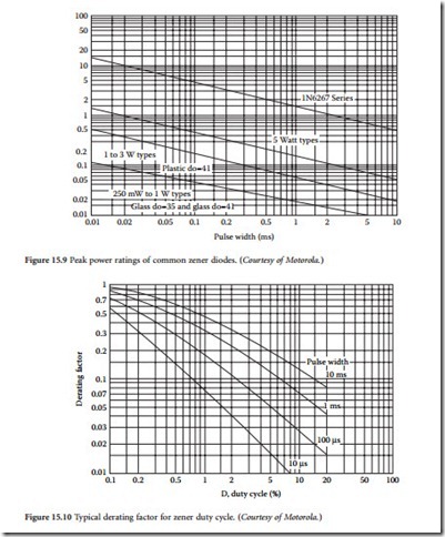
Most zeners handle less than their rated power during normal applications and are designed to oper- ate most effectively at this low level. Zener transient suppressors (such as the Motorola 1N6267 MoSorb series), sometimes known as silicon avalanche diodes (SADs), typically are designed to withstand rela- tively large, short-duration power pulses. This is accomplished by enlarging the chip and the effective junction area to withstand high-energy surges. Figure 15.9 charts the short-pulse surge capability of these devices. This data applies for nonrepetitive conditions with a lead temperature of 25°C.
It is necessary to determine the pulse width and peak power of the transient being suppressed when using Figure 15.9. This can be done by taking whatever waveform the transient is and approximating it with a rectangular pulse with the same peak power. For example, an exponential discharge with a 1 ms time constant can be approximated by a rectangular pulse 1 ms wide that has the same peak power as the transient. This would be a better approximation than a rectangular pulse 10 ms wide with a correspond- ingly lower amplitude because the heating effects of different pulse widths affect the power handling capability of the device, as can be observed in Figure 15.9. Such an approximation also represents a conservative approach because the exponential discharge will contain approximately one-half the energy of a rectangular pulse with the same pulse width and amplitude.
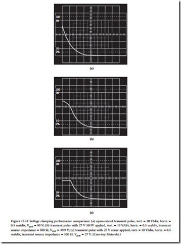
When used in repetitive applications, the peak power must be reduced as indicated by the curves given in Figure 15.10. Average power also must be derated as the lead or ambient temperature exceeds 25°C. The power derating curve normally given on data sheets can be normalized and used for this purpose.
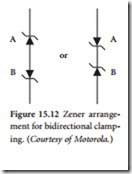
The clamping characteristics of zeners and MOVs are best compared by measuring their voltages under transient conditions. The waveform traces of Figure 15.11 are the result of a bench test performed to compare the clamping characteristics of a zener with those of a common MOV; both were 27 V devices. Waveform 6.11a shows the pulse generator output voltage, which synthesizes a common type of transient pulse. Waveforms 6.11b and c show the clamping voltages of the MOV and zener, respectively, with a surge source impedance of 500 Ω. As shown in the waveform traces, the zener suppressor has sig- nificantly better voltage-clamping characteristics than the MOV. The major tradeoff with using a zener- type suppressor is its cost-vs.-power handling capability.
If a transient is impressed on the circuit that exceeds the capabilities of the particular zener or MOV used, the load will still be protected because both devices fail in a short circuit. The theoretical reaction
time for a zener device is in the picosecond range, but this is slowed somewhat because of lead and pack- age inductance. For very fast rising transients, it is important, therefore, to minimize external inductances (resulting from wiring and other factors), which will minimize overshoot.
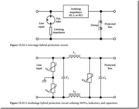
Connecting zeners in a back-to-back arrangement will enable bidirectional voltage-clamping characteristics, as illustrated in Figure 15.12. If devices A and B are of the same voltage rating, a transient of either polarity will be clamped at approximately that voltage (one zener will be reverse-bias mode while the other will be in the forward- or bias mode). When clamping low voltages, it may be necessary to con- B B sider the forward voltage drop of the forward-biased zener. Bipolar zener devices also are available as packaged components.
In almost every application, the transient suppression device is placed in parallel with the load, or in parallel with the component to be protected. Because the main purpose of the circuit is to clamp the voltage appearing across the load, the suppressor should be placed as close to the load as possible to minimize overshoot resulting from wiring (or other inductive) effects. Figure 15.13 illustrates the results of inductive overshoot.
When the zener is in the breakdown Transient mode of operation (e.g., when suppressing a transient), its effective capacitance increases drastically from what it was in the off-state. This makes the zener ideal for parallel pro- tection schemes because, during transient suppression, its large effective capacitance will tend to hold the voltage across the pro- tected element constant, while in the off Zener voltage state (normal conditions, no transient present), its low off-state capacitance will not attenuate high-frequency signals.
Hybrid Suppression Circuits
Any of the elements discussed so far in this chapter can be combined into a single hybrid unit to gain the best elements of each technology. A hybrid protector can be designed that will respond to several types of line disturbances. As shown in Figure 15.14, a gas tube commonly is combined with a silicon clamping device to provide two-stage suppression. When a transient hits, the clamping device will initially limit the voltage because of its faster response time, relative to the gas tube. The tube will then fire and crowbar the bulk of the energy. Proper matching of the gas tube and the clamping device is an important design parameter. If, for example, the tube is not presented with sufficient voltage to ensure that it fires, the silicon device will have to take the full surge energy, and may be destroyed in the process. The series imped- ance shown in the diagram can be a resistor or an inductor, or simply the interconnection impedance of the wiring system. It is sized to pass the full load current while still providing sufficient impedance to ensure that the tube will fire.
A multistage suppressor is shown in Figure 15.15. The circuit is composed primarily of metal-oxide varistors. VR1 and VR2 are the primary devices, and they absorb most of the overvoltage transients. Inductors L1 and L2 work with VR3 to exercise tight control over voltage excursions.
The response time of voltage-clamping devices is significantly affected by lead inductance. For this reason, lead lengths for all devices in a protection unit should be kept to a minimum.
