High-frequency power supplies
High-frequency power supplies or switched-mode power supplies are widely used to derive low-voltage dc supplies from the ac utility, and operate by first rectifying the ac input to provide high-voltage dc, which is then converted into high-frequency ac, typically at around 100 kHz, and then passed through a physically small high- frequency transformer, before finally being rectified and smoothed to form the output. Power levels range from a few watts to a few kilowatts.
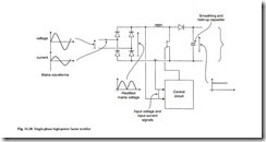
Traditionally, at these low power levels the input rectifier consists of a single-phase bridge and large smoothing capacitor, however in recent years this arrangement has become unacceptable for all but the very lowest power levels due to the high harmonic content of the currents drawn by such a rectifier circuit. The input current to the recti- fier consists of narrow pulses at the peaks of the ac voltage waveform. Instead of adding large low-frequency filters at the rectifier input, active high-power factor rectifiers are increasingly being used to provide high-quality, near-sinusoidal input currents by using high-frequency converter techniques. A common example, based on the boost converter, is illustrated in Fig. 11.18.
A full-wave rectified voltage waveform is presented as the input to the boost converter, which, through the use of an input current feedback loop, is controlled to offer a constant input resistance, that is, to draw an input current that follows the full- wave rectified voltage. As a result the input power factor is almost unity. However, a
small high frequency filter may be required at the input to provide a path for the high frequency inductor ripple current. To ensure proper operation, the boost converter output voltage must be maintained above the peak of the ac input, which is achieved by sizing the output capacitor to accommodate the twice mains frequency pulsation in power flow that occurs through the boost converter, and also by modulating the amplitude of the boost converter input current to compensate for changes in the power drawn from the power supply output.
High-frequency coupled dc–dc converter circuits that are commonly used in switched mode power supplies are the forward converter and the flyback converter, and these are briefly reviewed in the following sections.
Forward converter
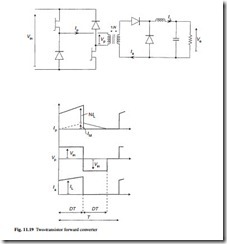
This is a transformer-isolated derivative of the buck converter, and the two circuits operate in a very similar manner. In the two-transistor version of the circuit, shown in Fig. 11.19, the devices operate in synchronism with a duty ratio D. The waveforms show a steady-state switching cycle, the transistors being turned on at the origin. The inductor current is assumed to be continuous with a small triangular ripple component. The waveforms show the primary voltage and current and the secondary current.
When the transistors turn on, the dc input voltage is applied to the primary wind- ing. The voltage is reflected across to the secondary winding multiplied by the turns ratio and acts to forward bias the series diode and reverse bias the freewheel diode; the inductor voltage is therefore given by NVin-Vo, causing a linear rise in the inductor current during the transistor on-time. The inductor current flows through the transformer secondary and is reflected through the turns ratio into the primary, transferring energy from the source. In addition the transformer magnetizing current rises linearly from zero.
When the transistors turn off, the inductor current diverts to the freewheel diode, the inductor voltage is equal to –Vo and the inductor current falls linearly. By equating the positive and negative inductor volt-seconds, the expression for the voltage conversion ratio is given in eqn 11.13:
The conversion ratio expression is similar to that of the buck converter, but is multi- plied by the transformer turns ratio.
When the transistors turn off, the stored energy in the transformer core acts to maintain the flow of magnetizing current, the conduction path being through the two diodes in the primary circuit and the dc source. As a result, the primary voltage reverses, the magnetizing current falls linearly, returning the stored magnetic energy to the dc source. Since the reverse voltage applied to the primary is equal in magnitude to the forward voltage, the current decays to zero in a time equal to the transistors on time. Therefore, for the magnetizing current to fall to zero before the start of the next cycle, the transistor duty ratio must be limited to a maximum of 0.5. The limitation on the duty ratio results in poor utilization of the transformer, power flowing through it only for up to 50 per cent of the time.
For applications of a few hundred watts, a single transistor circuit is sometimes used with a third winding to allow transformer reset, but this circuit has the disadvantage that the transistor off-state voltage becomes 2Vin. For higher powers, around 1 kW and above, a four-transistor full-bridge circuit (single-phase inverter) is used to drive
the transformer. This allows a true bidirectional voltage waveform to be impressed on the primary and enables power to flow through the transformer for almost 100 per cent of the cycle.
Flyback converter
This is often preferred at power levels below 100 W, where its simple circuit topology with only one magnetic component makes it the most economic solution. At higher power levels the circuit simplicity is out-weighed by the disadvantages of high ripple current in the output filter capacitor, high reverse voltages across the devices and poor utilization of the wound component.
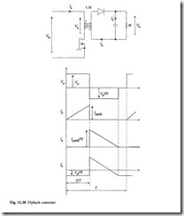
The circuit and waveforms are shown in Fig. 11.20. Here, Vp is the primary winding voltage, Ip the primary winding current, Is the secondary winding current, and Ic is the filter capacitor current. The currents in the magnetic component are assumed to be zero at the start of the cycle.
The turn-on instant is shown at the origin and when the transistor is conducting, the input voltage is impressed across the primary winding, causing a linear increase in cur- rent as energy is stored in the core and the flux increases. While the transistor is on, the secondary winding cannot conduct since the diode is reverse biased by a voltage NVin + Vo.
The primary current is rapidly reduced to zero as the transistor turns off, and to maintain the core flux a current starts to flow in the secondary winding. The second- ary current then falls linearly to zero as the stored magnetic energy is transferred to the load. It is important to note that the alternate conduction of the primary and secondary is quite different from the normal operation of a transformer, and results in the entire energy that passes through the circuit each cycle being stored momentarily in the core. The component is therefore known as a coupled inductor rather than a transformer, and due to the energy storage requirement, the coupled inductor tends to be significantly larger than a transformer designed for the same power and frequency.
The voltage conversion ratio for the converter may be obtained by equating the input and output energy per cycle as in eqn 11.14,
where Lp is the self-inductance of the primary winding and D is the transistor duty ratio. Re-arranging gives eqn 11.15.
The conversion ratio is a linear function of D, but also depends upon load, operating frequency and the primary inductance. Surprisingly the turns ratio N does not appear in eqn 11.15; this is because the converter operates by transferring a fixed packet of energy to the output each cycle, which is independent of N.
There is a wide range of standards covering the performance of power electronic equipment, particularly with regard to electromagnetic compatibility and safety. Some standards are generic whilst others apply to specific classes of equipment. Examples of the most common standards are listed in Table 11.1.


