Objectives
After studying this unit, the student will be able to:
• Discuss the operation of the operational amplifier (op amp)
• List the major types of connections for operational amplifiers
• Connect a level detector circuit using an op amp
• Connect an oscillator using an op amp
The operational amplifier, like the 555 timer, has become a very common component in indus trial electronic circuits. The operational amplifier, or op amp, is used in hundreds of applications. Different types of op amps are available for differ ent types of circuits. Some op amps use bipolar transistors for input while others use field-effect transistors. The advantage of field-effect transis tors is that they have an extremely high input impedance which can be several thousand meg ohms. As a result of this high input impedance, the amount of current needed to operate the am plifier is small. In fact, op amps that use field-ef fect transistors for the inputs are generally consid ered to require no input current.
The ideal amplifier would have an input impedance of infinity. With an input impedance of infinity, the amplifier would not drain power from the signal source; therefore, the strength of the signal source would not be affected by the ampli fier. The ideal amplifier would also have zero out put impedance. With zero output impedance, the amplifier could be connected to any load resi tance without causing a voltage drop inside the ampli fier. If it had no internal voltage drop, the amplifier would utilize 100% of its gain. Finally , the ideal amplifier would have unlimited gain. This would enable it to amplify any input signal as much as desired.
Although the ideal amplifier does not exist,
the op amp is close. In this unit the operation of an old op amp, the 741, is described as typical of all operational amplifiers. Other op amps may have different characteristics of input and output impedance, but the basic theory of operation is the same for all of them.
The 741 op amp uses bipolar transistors for the inputs. The input impedance is about 2 meg ohms, the output impedance is about 75 ohms, and the open loop, or maximum gain, is about 200,000. The 741 is impractical for use with such a high gain so negative feedback, which will be discussed later, is used to reduce the gain. For ex ample, assume that the amplifier has an output voltage of IS volts. If the input signal voltage is greater than 11200,000 of the output voltage, or 75 microvolts 
the amplifier will be driven to saturation at which point it will not operate.
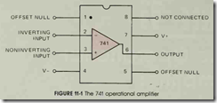
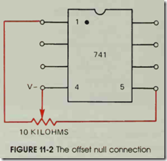
The 741 operational amplifier is usually housed in an eight-pin, in-line, integrated circuit package, figure 11-1. The op amp has two inputs called the inverting input and the noninverting in put. These inputs are connected to a differential amplifier which amplifies the difference between the two voltages. If both of these inputs are con nected to the same voltage, say by grounding both inputs, the output should be 0 volts. In actual practice, however, unbalanced conditions within the op amp may cause a voltage to be produced at the output. Since the op amp has a very high gain, a slight imbalance of a few microvolts at the input can produce several millivolts at the output. To counteract any imbalance, pins #1 and #5 are connected to the offset null which is used to pro duce 0 volts at the output. These pins are adjusted after the 741 is connected in a working circuit. To make the adjustments, a 10 kilohm potentiometer is connected across pins #1 and #5, and the wiper is connected to the negative voltage, fig ure 11-2.
Pin #2 is the inverting input. When a signal voltage is applied to this input, the output is in verted. For example, if a positive ac voltage is ap plied to the inverting input, the output will be a negative voltage, figure 11-3.
Pin #3 is the noninverting input. When a signal voltage is applied to the noninverting input, the output voltage is the same polarity. For ex ample, if a positive ac voltage is applied to the noninverting input, the output voltage will be pos itive also, figure 11-4.
Operational amplifiers are usually connected to above and below ground power supplies. Al though there are some circuit connections that do not require an above and below ground power supply, these are the exception instead of the rule. Pins #4 and #7 are the voltage input pins. Pin
#4 is connected to the negative, or below ground,
voltage and pin #7 is connected to the positive, or above ground, voltage.
The 741 operates on voltages that range from about 4 volts to 16 volts. Generally, the operating voltage for the 741 is 12 to 15 volts plus and mi nus. The 741 has a maximum power output rating of about 500 milliwatts.
Pin #6 is the output and pin #8 is not connected.
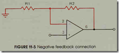
As stated previously, the open loop gain of the 741 operational amplifier is about 200,000. Since this amount of gain is not practical for most applications, something must be done to reduce the gain to a reasonable level. One of the great advantages of the op amp is the ease with which the gain can be controlled, figure ll-5. The amount of gain is controlled by a negative feed back loop. This is accomplished by feeding a por tion of the output voltage back to the inverting input. Since the output voltage is always opposite in polarity to the inverting input voltage, the amount of output voltage fed back to the input tends to reduce the input voltage. Negative feed back affects the operation of the amplifier in two ways: it reduces the gain; and it makes the ampli fier more stable.
The gain of the amplifier is controlled by the ratio of resistor R2 to resistor R1. If a noninvert ing amplifier is used, the formula 
is used to calculate the gain. If resistor R1 is 1 kilohm and resistor R2 is 10 kilohms, the gain of the amplifier is 11 
If the op amp is connected as an inverting amplifier, the input signal will be out of .pha e with the feedback voltage of the output. This will cause a reduction in the input voltage applied to the amplifier and in the gain. The formula 
is used to compute the gain of an inverting ampli fier. If resistor R1 is 1 kilohm and resistor R2 is 10 kilohms, the gain of the inverting amplifier is 10 
As a general rule, the 741 operational ampli fier is not operated above a gain of about 100 be cause it tends to become unstable at high gains. If more gain is desired, it is obtained by using more than one amplifier, figure ll-6. The output of one amplifier is fed into the input of another amplifier.
Another general rule for operating the 741 op amp is the total feedback resistance (Rl + R2) is kept at more than 1,000 ohms and less than 100,000 ohms. These rules apply to the 741 oper
ational amplifier but may not apply to other operational amplifiers .
BASIC CIRCUITS
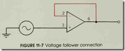
Op amps are generally used in three basic cir cuits that are used to build other circuits. One of these basic circuits is the voltage follower. In this circuit, the output of the op amp is connected di rectly back to the inverting input, figure 11-7. Since there is a direct connection between the out put of the amplifier and the inverting input, the gain of this circuit is 1. For example, if a signal voltage of .5 volts is connected to the noninverting input, the output voltage will be .5 volts also. You may wonder why anyone would want an amplifier that doesn’t amplify. Actually, this circuit does amplify something. It amplifies the input imped ance by the amount of the open loop gain. If the 741 has an open loop gain of 200,000 and an input impedance of 2 megohms, this circuit will give the amplifier an input impedance of 200 k X 2 meg or 400,000 megohms. This circuit connection is generally used for impedance matching purposes.
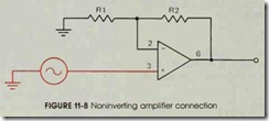
The second basic circuit is the noninverting amplifier, figure 11-8. In this circuit, the output voltage has the same polarity as the input voltage. If the input voltage is positive, the output voltage will be positive also. The formula 
is used to calculate the amount of gain in the neg ative feedback loop.
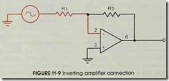
The third basic circuit is the inverting amplifier, figure 11-9. In this circuit the output voltage is opposite in polarity to the input voltage. If the input signal is positive, the output voltage will be negative at the same instant in time. The formula 
is used to calculate the amount of gain in this circuit.
CIRCUIT APPLICATIONS
The Level Detector
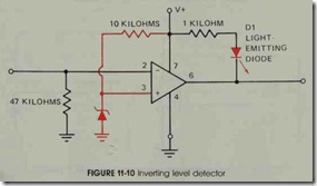
The operational amplifier is often used as a level detector or comparator. In this type of cir cuit, the 741 op amp is used as an inverted ampli fier to detect when one voltage becomes greater than another, figure 11-10. This circuit does not use above and below ground power supplies. In stead, it is connected to a power supply that has a single positive and negative output.
During normal operation, the noninverting input of the amplifier is connected to a zener diode which produces a constant positive voltage at the noninverting input of the amplifier. This constant positive voltage is used as a reference. As long as the noninverting input is more positive than the inverting input, the output of the amplifier is high.
A light-emitting diode (LED), D1, is used to detect a change in the polarity of the output. As long as the output of the op amp is high, the LED is turned off. When the output of the amplifier is high, the LED has equal voltage applied to its an ode and cathode. Since both the anode and cathode are connected to + 12 volts, there is no potential difference and, therefore, no current flow through the LED.
If the voltage at the inverting input becomes more positive than the reference voltage applied to pin #3, the output voltage will fall to about +2.5 volts. The output voltage of the op amp will not fall to 0 or ground in this circuit because the op amp is not connected to a voltage that is below ground. To enable the output voltage to fall to 0 volts, pin #4 must be connected to a voltage be low ground. When the output drops, a potential of about 9.5 volts (12 – 2.5 = 9.5) is produced across R1 and Dl. The lowering of potential causes the LED to turn on, which indicates that the op amp’s output has changed from high to low.
In this type of circuit, the op amp appears to be a digital device in that the output seems to have only two states, high and low. But, the op amp is not a digital device. This circuit only makes it ap pear to be digital. In figure 11-10, there is no neg ative feedback loop connected between the output and the inverting input. Therefore, the amplifier uses its open loop gain, which is about 200,000 for the 741, to amplify the voltage difference between the inverting input and the noninverting input. If the voltage applied to the inverting input be comes 1 millivolt more positive than the reference voltage applied to the noninverting input, the amplifier will try to produce an output that is 200 volts more negative than its high state voltage (.001 x 200,000 = 200). The output voltage of the amplifier cannot be driven 200 volts more negative, though, because only 12 volts are ap plied to the circuit. Therefore, the output voltage reaches the lowest voltage it can and goes into sat uration. This causes the op amp to act like a digi tal device.
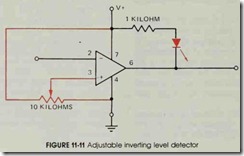
If the zener diode is replaced with a voltage divider as shown in figure 11-11, the reference voltage can be set to any value by adjusting the variable resistor. For example, if the voltage at the noninverting input is set for 3 volts, the output of the op amp will go low when the voltage applied to the inverting input becomes greater than + 3 volts. If the voltage at the noninverting input is set for 8 volts, the output voltage will go low when the voltage applied to the inverting input becomes
greater than + 8 volts. In this circuit the output of the op amp can be manipulated through the adjustment of the noninverting input.
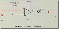
In the two circuits just described, the op amp’s output shifted from a high level to a low level. There may be occasions, however, when the output must be changed from a low level to a high level. This can be accomplished by connecting the inverting input to the reference voltage, and the noninverting input to the voltage being sensed, figure 11-12. In this circuit, the zener diode is used to supply a positive reference voltage to the inverting input. As long as the voltage at the inverting input is more positive than the voltage at the noninverting input, the output voltage of the op amp will be low. If the voltage applied to the noninverting input becomes more positive than the reference voltage, the output of the op amp will become high.
Depending on the application, this circuit could cause a small problem. As stated previously, since this circuit does not use an above and below ground power supply, the low output voltage of
the op amp is about +2.5 volts. This positive output voltage could cause any other devices con nected to the op amp’s output to be on when they should be off. For instance, if the LED shown in figure 11-12 is used, it will glow dimly even when the output is in the low state.
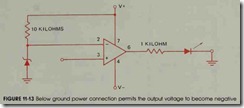
One way to correct this problem is to connect the op amp to an above and below ground power supply as shown in figure 11-13. In this circuit, the output voltage of the op amp is negative or below ground as long as the voltage applied to the inverting input is more positive than the voltage applied to the noninverting input. When the out put voltage of the op amp is negative with respect to ground, the LED is reverse biased and cannot operate. If the voltage applied to the noninverting input becomes more positive than the voltage ap plied to the inverting input, the output of the op amp will become positive and the LED will turn on.
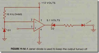
Another method of correcting the output voltage problem is shown in figure 11-14. In this circuit, the op amp is connected again to a power supply that has a single positive and negative out put. A zener diode, D2, is connected in series with the output of the op amp and the LED. The voltage value of diode D2 is greater than the out put voltage of the op amp in its low state, but less than the output voltage of the op amp in its high state. For instance, assume that the value of zener diode D2 is 5.1 volts. If the output voltage of the op amp in its low state is 2.5 volts, diode D2 will
not conduct. If the output voltage becomes + 12 volts when the op amp switches to its high state, diode D2 will turn on and conduct current to the LED. The zener diode, D2, keeps the LED com pletely off until the op amp switches to its high state providing enough voltage to overcome the reverse voltage drop of the zener diode.
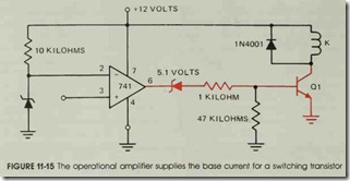
In the preceding circuits, an LED was used to indicate the output state of the amplifier. Keep in mind that the LED is used only as a detector, while the output of the op amp can be used to control almost anything. For example, the output of the op amp can be connected to the pase of a transistor as shown in figure 11-15. The transistor can then control the coil of a relay which could, in turn, control almost anything.
The Oscillator
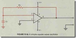
The operational amplifier can be used as an oscillator. The simple circuit shown in figure 11-16 produces a square wave output. However, this circuit is impractical because it depends on a slight imbalance in the op amp, or random circuit noise to start the oscillator. A voltage difference of a few millivolts between the two inputs is all that is needed to raise or lower the output of the am plifier. For example, if the inverting input be comes slightly more positive than the noninverting input, the output will go low or become negative. When the output is negative, capacitor CT charges through resistor RT to the negative value of the output voltage. When the voltage applied to the inverting input becomes slightly more negative than the voltage applied to the noninverting input, the output changes to a high, or positive, value of voltage. When the output is positive, capacitor CT charges through resistor RT toward the positive output voltage.
This circuit would work well if there were no imbalance in the op amp, and if the op amp were shielded from all electrical noise. In practical ap plication, however, there is generally enough im balance in the amplifier or enough electrical noise to send the op amp into saturation, which stops the operation of the circuit.
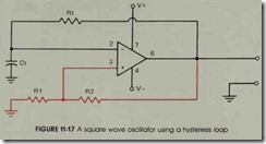
The problem with this circuit is that a milli volt difference between the two inputs is enough to drive the amplifier’s output from one state to the other. This problem can be corrected by the addition of a hysteresis loop connected to the non inverting input as shown in gure 11-17. Resistors R1 and R2 form a voltage divider for the nonin verting input. These resistors generally have equal value. To understand the circuit operation, as sume that the inverting input is slightly more pos itive than the noninverting input. This causes the output voltage to be negative. Also assume that the output voltage is negative 12 volts as compared to ground. If resistors R1 and R2 have equal value, the noninverting input is driven to -6 volts by the voltage divider. Capacitor CT begins to charge through resistor RT to the value of the out put voltage. When capacitor CT has been charged to a value slightly more negative than the -6 volts applied to the noninverting input, the op amp’s
output rises to + 12 volts above ground. When the output of the op amp changes from -12 volts to + 12 volts, the voltage applied to the noninverting input changes from -6 volts to +6 volts. Capac itor CT now begins to charge through resistor RT
to the positive voltage of the output. When the voltage applied to the inverting input becomes more positive than the voltage applied to the non inverting input, the output changes to -12 volts. The voltage applied to the noninverting input is
driven from +6 volts to -6 volts, and capacitor
CT again begins to charge toward the negative output voltage of the op amp.
The addition of the hysteresis loop has greatly changed the operation of the circuit. The voltage differential between the two inputs is now volts instead of millivolts. The output frequency of the oscillator is determined by the values of CT and RT. The period of one cycle can be computed by using the formula T = 2RC.
The Pulse Generator
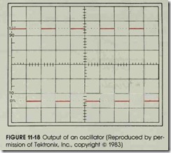
The operational amplifier can be used as a pulse generator. The difference between an oscil lator and a pulse generator is the period of time the output is on compared to the period of time it is low or off. For instance, an oscillator is gener ally considered to produce a waveform that has positive and negative pulses of equal voltage and
time, figure 11-18. The positive value of voltage is the same as the negative value, and the positive and negative cycles are turned on for the same amount of time. This waveform is produced when an oscilloscope is connected to the output of a square wave oscillator.
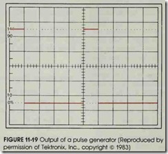
If the oscilloscope is connected to a pulse gen erator, however, a waveform similar to the one shown in figure 11-19 will be produced. The pos itive value of voltage is the same as the negative value just as it was in figure 11-18, but the positive pulse is of a much shorter duration than the neg ative pulse.
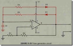
The 741 operational amplifier can easily be changed from a square wave oscillator to a pulse generator, figure 11-20. The pulse generator circuit is the same basic circuit as the square wave oscillator with the addition of resistors R3 and R4, and diodes D1 and D2. This circuit permits ca pacitor CT to charge at a different rate when the output is high, or positive, than when the output is low, or negative. For instance, assume that the voltage of the op amp’s output is – 12 volts. When the output voltage is negative, diode D1 is reverse biased and no current can flow through re sistor R3. Therefore, capacitor CT must charge through resistor R4 and diode D2 which is for ward biased. When the voltage applied to the in verting input becomes more negative than the voltage applied to the noninverting input, the out put voltage of the op amp rises to + 12 volts. When the output voltage is + 12 volts, diode D2 is reverse biased and diode D 1 is forward biased. Therefore, capacitor CT begins charging toward the + 12 volts through resistor R3 and diode Dl. The amount of time the output of the op amp is low is determined by the value of CT and R4, and the amount of time the output remains high is de termined by the value of CT and R3. The ratio of the amount of time the output voltage is high to the amount of time it is low can be determined by the ratio of resistor R3 to resistor R4.
REVIEW QUESTIONS
1. When the voltage connected to the inverting input is more positive than the voltage connected to the noninverting input, will the output be positive or negative?
2. What is the input impedance of a 741 operational amplifier?
3. What is the average open loop gain of the 741 operational amplifier?
4. What is the average output impedance of the 741 operational amplifier?
5. Operational amplifiers are commonly used in what three connections?
6. When the operational amplifier is connected as a voltage follower, it has a gain of 1 (one). If the input voltage is not amplified, what is?
7. Name two effects of negative feedback.
8. Refer to figure 11-8. If resistor R1 is 200 ohms and resistor R2 is 10 kilohms, what is the gain of the amplifier?
9. Refer to figure 11-9. If resistor R1 is 470 ohms and resistor R2 is 47 kilohms,
what is the gain of the amplifier?
10. What is the purpose of the hysteresis loop when the op amp is used as an oscillator?
