Diode Biasing
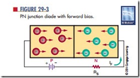
When a voltage is applied to a diode, it is referred to as a bias voltage. Figure 29-3 shows a P–N junction diode connected to a voltage source. A resistor is added for limiting current to a safe value.
In the circuit shown, the negative terminal of the voltage source is connected to the N-type material. This forces electrons away from the terminal, toward the P–N junction. The free electrons that accumulate on the P side of the junction are attracted by the positive terminal. This action cancels the negative charge on the P side; the barrier voltage is eliminated, and a current is able to flow. Current flow occurs only if the external voltage is greater than the barrier voltage.
The voltage source supplies a constant flow of electrons, which drift through the N-type material along
with the free electrons contained in it. Holes in the P material also drift toward the junction. The holes and electrons combine at the junction and appear to cancel each other. However, as the electrons and holes com- bine, new electrons and holes appear at the terminals of the voltage source. The majority carriers continue to move toward the P–N junction as long as the voltage source is applied.
Electrons flow through the P side of the diode, attracted by the positive terminal of the voltage source. As electrons leave the P material, holes are created that drift toward the P–N junction, where they combine with other electrons. When the current flows from the N-type toward the P-type material, the diode is said to have a forward bias.
The resistance of the P and N materials and the external resistance of the circuit limits the cur- rent that flows when a diode is forward biased. The diode resistance is small. Therefore, connecting a voltage directly to a forward-biased diode creates a large current flow. This can generate enough heat to destroy the diode. To limit the forward current flow, an external resistor must be connected in series with the diode.
A diode conducts current in the forward direction only if the external voltage is larger than the barrier voltage and is connected properly. A germanium diode requires a minimum forward bias of 0.3 V; a silicon diode requires a minimum forward bias of 0.7 V.
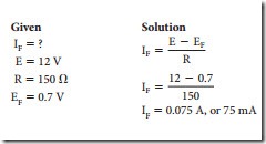
Once a diode starts conducting, a voltage drop occurs. This voltage drop is equal to the barrier voltage and is referred to as the forward voltage drop (EF). The voltage drop is 0.3 V for a germanium diode and 0.7 V for a silicon diode. The amount of forward current (IF) is a function of the external voltage (E), the forward voltage drop (EF), and the external resistance (R). The relationship can be shown using Ohm’s law:
EXAMPLE: A silicon diode has an external bias voltage of 12 V with an external resistor of 150 V. What is the total forward current?
age current. In germanium diodes, it is measured in microamperes; in silicon diodes, it is measured in nanoamperes. Germanium has more leakage current
In a diode that is forward biased, the negative terminal of the external voltage source is connected to the N material, and the positive terminal is connected to the P material. If these terminals are reversed, the diode does not conduct and is said to be connected in reverse bias (Figure 29-4). In this configuration, the free electrons in the N material are attracted toward the positive terminal of the external voltage source. This increases the number of positive ions in the area of the P–N junction, which increases the width of the depletion region on the N side of the junction. Electrons also leave the negative terminal of the voltage source and enter the P material. These electrons fill holes near the P–N junction, causing the holes to move toward the negative terminal, which increases the width of the depletion region on the P side of the junction. The overall effect is that the depletion region is wider than in an unbiased or forward-biased diode.
The reverse-biased voltage increases the barrier voltage. If the barrier voltage is equal to the external voltage source, holes and electrons cannot support current flow. A small current flows with a reverse bias applied. This leakage current is referred to as reverse current (iR) and exists because of minority carriers. At room temperature, the minority carriers are few in number. As the temperature increases, more because it is more sensitive to temperature. This disadvantage of germanium is offset by its smaller barrier voltage.
In summary, a P–N junction diode is a one-direc- tional device. When it is forward biased, a current flows. When it is reverse biased, only a small leakage current flows. It is this characteristic that allows the diode to be used as a rectifier. A rectifier converts an AC voltage to a DC voltage.
Questions
1. What is a bias voltage?
2. What is the minimum amount of voltage needed to produce current flow across a P–n junction diode?
3. What is the total forward current for a germanium diode with a 9 V external bias voltage and a 180 V external resistor?
4. What is the difference between forward and reverse biasing?
5. What is leakage current in a P–n junction diode?


