SINGLE-CORE MICROPROCESSOR UNITS
A microprocessor incorporates most of the entire central processing functions on a single inte- grated circuit (IC). The first microprocessors emerged in the early 1970s, and were used for electronic calculators. Since then, microprocessors within personal computers and industrial embedded controllers have evolved continuously, with each version being compatible with its predecessors.
The major producers of microprocessors have been Intel (Integrated Electronics Corporation) and AMD (Advanced Micro Devices, Inc.) since the early 1970s. Intel marketed the first microprocessor in 1971, named the 4004, a revolution in the electronics industry. With this processor, functionality started to be programmed by software. Am2900 is a family of integrated circuits (ICs) created in 1975 by AMD. They were constructed with bipolar devices, in a bit-slice topology, and were designed to be used as modular components, each representing a different aspect of a computer’s central processing unit (CPU).
At first, these microprocessors only handled 4 bits of data at a time (a nibble), contained 2000 transistors, had 46 instructions, and allowed 4 kB of program code and 1 kB of data, and had speeds of around several MHz. However, both Intel, AMD and other corporations such as IBM and Motorola quickly expanded the microprocessors’ capacities from 8, 10, 14, 16, 20, 24, 32, 64, 128 into the 256 bits of current versions; increased their transistors from 2000 into thousands of millions; and enhanced their speeds from a few MHz into a few hundred or more GHz. At the same time personal computers and industrial controllers have been developed that use these advanced microprocessors.
Microprocessors come and go, but most manufacturers know that the important differences between them are often microprocessor clock speeds and cache sizes. Although the performance of today’s microprocessors continues to improve, existing architectures based on an out-of-order execution model require increasingly complex hardware mechanisms and are increasingly impeded by performance limiters such as branches and memory latency. In the mid-1980s to early-1990s, a crop of new high-performance RISC (reduced instruction set computer) microprocessors ap- peared with discrete RISC-like designs such as the IBM 801 and others. RISC microprocessors were initially used in special-purpose machines and UNIX workstations, but then gained wide acceptance in other roles. As of 2007, two 64-bit RISC architectures were still being produced in volume for non-embedded applications; SPARC and Power Architecture. The RISC-like Itanium is produced in smaller quantities. The vast majority of 64-bit microprocessors are now x86-64 CISC designs from AMD and Intel.
Though the term “microprocessor” has traditionally referred to a single-core (chipset) or multicore (chipset) CPU or system-on-a-chip (SoC), several types of specialized processing devices have followed from the technology. The most common examples are microcontrollers, digital signal processors (DSP) and graphics processing units (GPU). Many of these are either not programmable, or have limited programming facilities. For example, in general, GPUs through the 1990s were mostly non-programmable and have only recently gained limited facilities such as programmable vertex shaders. There is no universal consensus on what defines a “micropro- cessor”, but it is usually safe to assume that the term refers to a general-purpose CPU of some sort, and not a special-purpose processor unless specifically noted. The latest ones have a unique combination of innovative features, including explicit parallelism, prediction, and speculation, which are described below.
(1) Parallelism
In today’s microprocessor architectures, the compiler creates sequential machine codes that attempt to mimic parallelism in hardware. The microprocessor’s hardware must then reinterpret this machine code and try to identify opportunities for parallel execution; the key to faster performance. This process is inefficient not only because the hardware does not always interpret the compiler’s intentions correctly, but also because it uses a valuable die area that could be better used to do real work such as executing instructions. Even today’s fastest and most efficient microprocessors devote a significant percentage of hardware resources to this task of extracting more parallelism from software code.
The use of explicit parallelism enables far more effective execution of software instructions. In the newer architecture models, the compiler analyzes and explicitly identifies parallelism in the software at compile time. This allows optimal structuring of machine code to deliver the maximum performance before the processor executes it, rather than potentially wasting valuable microprocessor cycles at runtime. The result is significantly improved processor utilization, and no precious die area is wasted by the hardware reorder engine, as occurs in out-of-order reduced instruction set computer (RISC) processors.
(2) Prediction
Simple decision structures, or code branches, are a hard performance challenge to out-of-order RISC architectures. In the simple if-then-else decision code sequence, traditional architectures view the code in four basic blocks. In order to continuously feed instructions into the processor’s instruction pipe- line, a technique called branch prediction is commonly used to predict the correct path. With this tech- nique, mispredicts commonly occur 5 10% of the time, causing the entire pipeline to be purged and the correct path to be reloaded. This level of misprediction can slow processing speed by as much as 30 40%.
To address this problem, and to improve performance, the new architectures use a technique known as prediction. Prediction begins by assigning special flags called predicate registers to both branch paths p1 to the “then” path and p2 to the “else” path. At run time, the compare statement stores either a true or a false value in the 1-bit predicate registers. The microprocessor then executes both paths but only the results from the path with a true predicate flag are used. Branches, and the possibility of associated mispredicts, are removed, the pipeline remains full, and performance is increased accordingly.
(3) Speculation
Memory latency is another big problem for current microprocessors’ architectures. Because memory speed is significantly slower than processor speed, the microprocessor must attempt to load data from memory as early as possible to ensure that data are available when needed. Traditional architectures allow compilers and microprocessor to schedule loads before data are needed, but branches act as barriers to this load hoisting.
The new architectures employ a technique known as “speculation” to initiate loads from memory earlier in the instruction stream, even before a branch. Because a load can generate exceptions, a mechanism to ensure that exceptions are properly handled is needed to support speculation that hoists loads before branches. The memory load is scheduled speculatively above the branch in the instruction stream, so as to start memory access as early as possible. If an exception occurs, this event is stored and the “checks” instruction causes the exception to be processed. The elevation of the load allows more time to deal with memory latency, without stalling the processor pipeline. Branches occur with great frequency in most software code sequences. The unique ability of these architectures to schedule loads before branches significantly increases the number of loads that can be speculated in comparison with traditional architectures.
5.1.1 Microprocessor unit organization
The microprocessor plays a significant role in the functioning of industries everywhere. Nowadays, the microprocessor is used in a wide range of devices or systems as a digital data processing unit, or as the computing unit of an intelligent controller or a computer to control processes, or make production automated, and even to turn devices on or off. The microprocessor is a multipurpose, programmable, clock-driven, register-based electronic device that reads binary instructions from a storage device called memory, accepts binary data as input and processes this data according to those instructions, and provides results as output. At a very elementary level, an analogy can be drawn between micropro- cessor operations and the functions of the human brain, which processes information according to understandings (instructions) stored in its memory. The brain gets input from the eyes and ears and sends processed information to output “devices”, such as the face with its capacity to register expression, the hands, or the feet.
A typical programmable machine can be represented by five components; microprocessor, memory, input, output, and bus. These five components work collaboratively and interactively with each other to perform a given task; thus they comprise a system. The physical components are called hardware. A set of instructions written for the microprocessor to perform a task is called a program, and a group of programs is called software. Assuming that a program and data are already entered in the memory, the microprocessor executes a program by reading all the data including instructions from the memory via the bus, and then processes these data in terms of the instructions, then writes the result into memory via the bus.
(1) Block diagram of a microprocessor unit
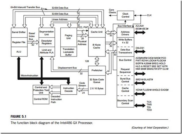
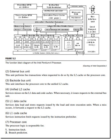
Figure 5.1 depicts a function block diagram of the Intel-486 GX processor chipset, which gives the microarchitecture of this Intel processor. Figure 5.2 is the block diagram for the microarchitecture of the Intel Pentium-4 processor chipset.
(2) Microprocessor
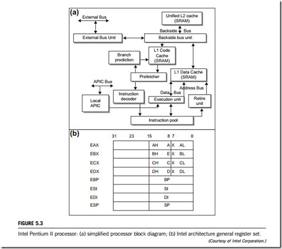
The Pentium series of microprocessors made by Intel, up to now, includes the Pentium Pro, the Pentium II, the Pentium III, and the Pentium 4, etc. As shown in Figure 5.3(a), the Pentium Pro consists of the following basic hardware elements:
(1) Intel Architecture registers
The Intel Architecture register set implemented in the earlier 80×86 microprocessor is extremely small. This small number of registers permits the processor (and the programmer) to keep only a small number of data operands close to the execution units, where they can be accessed quickly. Instead, the programmer is frequently forced to write back the contents of one or more of the processor’s registers to memory when additional data operands need to be read from memory in order to be operated on. Later, when the programmer requires access to the original set of data operands, they must again be read from memory. This juggling of data between the register set and memory takes time and exacts a penalty on the performance of the program. Figure 5.3(b) illustrates the Intel Architecture general register set.
3. Parsing of Intel Architecture instruction stream.
4. Decoding of Intel Architecture instructions into RISC instructions that are referred to as micro-ops or u-ops.
5. Mapping accesses for Intel Architecture register set to a large physical register set.
6. Dispatch, execution, and retirement of micro-ops.
(8) Local advanced programmable interrupt controller (APIC) unit
The APIC is responsible for receiving interrupt requests from other processors, the processor local interrupt pins, the APIC timer, APIC error conditions, performance monitor logic, and the IO APIC module. These requests are then prioritized and forwarded to the processor core for execution.
(9) Processor startup
At startup, upon the desertion of reset and the completion of a processor’s BIST bit of the configuration register, the processor must wake up and start fetching, decoding, and executing the power-on self test (POST) code from the ROM (read-only memory). The Intel multiprocessing specification (available for download at the Intel developers’ website) dictates that the startup code executed by the processor is responsible for detecting the presence of all the components on the processor chipset. When the available components have been detected, the startup code stores this information as a table in nonvolatile memory. According to this specification, both the BIOS code and the POST code are responsible for detecting the presence of and initializing the components. Intel recommends that both the POST code and the BIOS code initialize a predefined RAM location to 1hex. This location is referred to as the central processing unit (CPU) counter.
(10) The fetch, decode, execute engine
At the heart of the processor are the execution units that execute instructions. As shown in Figure 5.3 (a), the processor includes a fetch engine that attempts to properly predict the path of program execution and generates an ongoing series of memory-read operations to fetch the desired instructions.
The high-speed (e.g., 200 MHz or 1.5 GHz) processor execution engine is then bound by the speed of external memory accesses. It should be obvious that it is extremely advantageous to include a very high- speed cache memory on board so that the processor keeps copies of recently used information of both code and data. Memory-read requests generated by the processor core are first submitted to the cache for a lookup before being propagated to the external bus in an event of cache miss.
Pentium processors include both a code cache and a data cache in the level 1 cache. In addition, they include a level 2 cache tightly coupled to the processor core via a private bus. The processor’s caches are disabled at power-up time, however. In order to realize the processors’ full potential, the caches must be enabled. The steps for the Pentium processors to execute instructions are briefly described below:
1. Fetch Intel Architecture instructions from memory in strict program order.
2. Decode, or translate, them in, also strict program order, into one or more fixed-length RISC instructions known as micro-ops or u-ops.
3. Place the micro-ops into an instruction pool in strict program order.
4. Until this point, the instructions have been kept in original program order. This part of the pipeline is known as the in-order front end. The processor then executes the micro-ops in any order possible as the data and execution units required for each micro-op become available. This is known as the out-of-order portion of pipeline.
5. Finally, the processor commits the results of each micro-op execution to the processor’s register set in the order of the original program flow. This is the in-order rear end.
The new Pentium processors implement dynamic execution microarchitecture, a combination of multiple branch prediction, speculation execution, and data flow analysis. These Pentium processors execute MMX (which will be detailed in a subsequent paragraph) technology instructions for enhanced media and communication performance.
Multiple branches predict the flow of the program through several branches. Use of a branch prediction algorithm enables the processor to anticipate jumps in instruction flow. It predicts where the next instruction can be found in memory with a 90% or greater accuracy. This is made possible because the processor is fetching instructions, and at the same time it is also looking at instructions further ahead in the program.
Data flow analysis analyzes and schedules instructions to be executed in an optimal sequence, independent of the original program order; the processor looks at decoded software instructions and determines whether they are available for processing or whether they are dependent on other instructions.
Speculative execution increases the rate of execution by looking ahead of the program counter and executing instructions that are likely to be needed later. When the processor executes several instructions at a time, it does so using speculative execution. The instructions being processed are based on predicted branches and the results are stored as speculative results. Once their final state can be determined, the instructions are returned to their proper order and committed to permanent machine state.
(11) Processor cache
Figure 5.3(a) provides an overview of the processor’s cache, showing its two types; data cache and code cache. The L1 code cache services the requests for instructions generated by the instruction prefetcher (the prefetcher is the only unit that accesses the code cache and it only reads from it, so the code cache is read only), whereas the L1 data cache services memory data read and write requests generated by the processor’s execution units when they are executing any instruction that requires a memory data access. The unified L2 cache resides on a dedicated bus referred to as the backside bus. It services misses on the L1 caches, and, in the event of an L2 miss, it issues a transaction request to the external memory. The information is placed in the L2 cache and is also forwarded to the appropriate L1 cache for storage.
The L1 data cache services read and writes requests initiated by the processor execution units. The size and structure of the L1 data cache is processor implementation-specific. As processor core speeds increase, cache sizes will increase to service the greater need for memory access. Each of the data cache’s cache banks, is further divided into two banks. When performing a lookup, the data cache views memory as divided into pages equal to the size of one of its cache banks (or ways). Furthermore, it views each memory page as having the same structure as one of its cache ways. The target number is used to index into the data cache directory, and select a set of two entries to compare against. If the target page number matches the tag field in one of the entries in the E, S, or M state given below, it is a cache hit. The data cache has a copy of the target line from the target page. The action taken by the data cache depends on whether or not the data access is a read or a write, the current state of the line, and the rules of conduct defined for this area of memory. Each line storage location within the data cache can currently be in one of four possible states:
1. Invalid state (I); there is no valid line in the entry.
2. Exclusive state (E); the line in the entry is valid, is still the same as memory, and no other processor has a copy of the line in its caches.
3. Shared state (S); the line in the entry is valid, still the same as memory, and one or more processors may also have copies of the line or may not because the processor cannot discriminate between reads by processors and reads performed by other, noncaching entries such as a host/PCI bridge.
4. Modified state (M); the line in the entry is valid, has been updated by this processor since it was
read into the cache, and no other processor has a copy of the line in its caches. The line in memory is stable.
The L1 code cache exists only to supply requested code to the instruction prefetcher. The prefetcher issues only read requests to the code cache, so it is a read-only cache. A line stored in the code cache can only be one of two possible states, valid or invalid, implemented as the S and I states. When a line of code is fetched from memory and is stored in the code cache, it consists of raw code. The designers could have chosen to prescan the code stream as it is fetched from memory and store boundary markers in the code cache to demarcate the boundaries between instructions within the cache line. This would preclude the need to scan the code line as it enters the instruction pipeline, but this would bloat the size of the code cache. Note that the Pentium’s code cache stores boundary markers. When performing a lookup, the code cache views memory as divided into pages equal to the size of one of its cache banks (or ways). Furthermore, it views each memory page as having the same structure as one of its cache ways.
(12) MMX technology
Intel’s Matrix Math Extensions (MMX) technology is designed to accelerate multimedia and communication applications whilst retaining full compatibility with the original Pentium processor. It contains five architectural design enhancements:
1. New instructions.
2. Single Instruction Multiple Data (SIMD). The new instructions use a SIMD model, operating on several values at a time. Using the 64-bit MMX registers, these instructions can operate on eight bytes, four words, or two double words at once, greatly increasing throughout.
3. More cache. Intel has doubled on-chip cache size to 32k. Hence, more instructions and data can be tored on the chip, reducing the number of times the processor needs to access the slower, off-chip memory area for information.
4. Improved branch prediction. The MMX processor contains four prefetch buffers, which can holdup to four successive code streams.
5. Enhanced pipeline and deeper write buffers. An additional pipeline stage has been added, and four write buffers are shared between the dual pipelines, to improve memory write performance.
MMX technology uses general-purpose, basic, instructions that are fast and easily assigned to the parallel pipelines in Intel processors. By using this general-purpose approach, MMX technology provides performance that will scale well across current and future generations of Intel processors. The MMX instructions cover several functional areas including:
1. Basic arithmetic operations such as add, subtract, multiply arithmetic shift, and multiply add.
2. Comparison operations.
3. Conversation instructions to convert between the new data types pack data together and unpack from small to larger data types.
4. Logical operations such as AND, NOT, OR, and XOR.
5. Shift operations.
6. Data transfer (MOV) instructions for MMX register-to-register transfers, or 64-bit and 32-bit load and store to memory.
The principal data type of the MMX instruction set is the packed, fixed-point integer, where multiple integer words are grouped into single 64-bit quantities. These quantities are moved to the 64-bit MMX registers. The decimal point of the fixed-point values is implicit, and is left for the programmer to control for maximum flexibility. Arithmetic and logical instructions are designed to support the different packed integer data types. These instructions have a different op code for each data type supported. As a result, the new MMX technology instructions are implemented with 57 op codes. The supported data types are signed and unsigned fixed-point integers, bytes, words, double words, and quad words. The four MMX technology data types are:
1. packed bytes: 8 bytes packed into one 64-bit quantity;
2. packed word: four 16-bit words packed into one 64-bit quantity;
3. packed double word: two 32-bit double words packed into one 64-bit quantity;
4. quad word: one 64-bit quantity.
From the programmer’s point of view, there are eight new MMX registers (MM0 MM7), along with new instructions that operate on these registers. But to avoid adding new states, these registers are mapped onto the existing floating-point registers (FP0 FP7). When a multitasking operating system (or application) executes an FSAVE instruction, e.g. to save state, the contents of MM0 MM7 are saved in place of FP0 FP7 if MMX instructions are in use.
Detecting the existence of MMX technology on an Intel microprocessor is done by executing the CPUID instruction and checking a set bit. Therefore, when installing or running, a program can query the microprocessor to determine whether or not MMX technology is supported, and proceed according to the result.
(3) Internal bus system
Figures 5.1 and 5.3(a) show that the internal bus systems of an Intel microprocessor, based on their functions, comprises the types below, each of them monitored by a corresponding bus controller or bus unit:
1. Backside bus.
2. Displacement bus.
3. APIC bus.
4. Cache buses, divided into data bus and address bus.
5. CPUs’ cluster bus.
(4) Memories
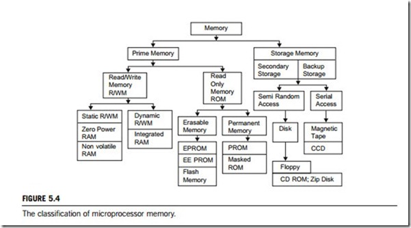
Memories on microprocessor chipsets can be classified into two groups; prime (system or main) memory and storage memory. The read/write memory (R/WM) and read-only memory (ROM) are examples of prime memory the memory the microprocessor uses in executing and storing programs. This memory should be able to keep up with the execution speed of the microprocessor, so it should be random access memory, meaning that the microprocessor should be able to access information from any register with the same speed (independent of its place in the chip). The size of a memory chip is specified in terms of bits. For example, a 1k memory chip means it can store 1k (1024) bits (not bytes). On the other hand, system memory in a PC is specified in bytes so 4M memory means it is 4 megabytes in size.
The other group is the storage memory, which uses devices such as magnetic disks and tapes (see Figure 5.4). This memory is used to store programs and results after the completion of program execution. Such storage is nonvolatile, meaning information remains intact even if the system power is turned off. The microprocessor cannot access programs stored in these devices directly; they need to be copied into the R/W prime memory first. Hence, the size of the prime memory, determines how large
a program the system can process. Storage memory is unlimited in size; when one disk is full, the next one can be used.
Figure 5.4 shows that these are also two types of storage memory; secondary storage and backup storage, which includes devices such as disks, magnetic tapes, etc. Prime (system) memory is divided into two main groups: read/write memory (R/WM) and read-only memory (ROM); each group includes several different types of memory, as discussed below.
(1) Read/write memory (R/WM)
As the name suggests, the microprocessor can write into or read from this memory; it is popularly known as random access memory (RAM). It is used primarily for information that is likely to be altered, such as writing programs or receiving data. This memory is volatile, meaning that when the power is turned off, all the contents are lost. Two types of R/W memories, static and dynamic are available; they are described in the following paragraphs.
1. Static memory (SRAM). This memory is made up of flip-flops, and it stores each bit as a voltage.
Each memory cell requires six transistors, so the memory chip has low density but high speed. SRAM, known as cache memory, resides on the processor chip. A high-speed cache is also included, external to the processor to improve the performance of a system.
2. Dynamic memory (DRAM). This memory is made up of MOS transistor gates, and it stores each bit as
a charge. In dynamic memory, stored information needs to be read and then written again every few milliseconds. It is generally used when system memory is at least 8k; for smaller systems, static memory is more appropriate. Various techniques are used to increase the speed of DRAM, which have resulted in the production of high-speed memory chips, such as Extended Data Out (EDO), Synchronous DRAM (SDRAM), and Rambus DRAM (RDRAM).
(2) Read-only memory (ROM)
ROM is nonvolatile memory; it retains stored information even if the power is turned off. This memory is used for programs and data that need not be altered. As the name suggests, the information can only be read, which means once a bit pattern is stored, it is permanent or at least semi-permanent. The permanent group also includes two types of memory; masked ROM and PROM, as does the semi-permanent group; EPROM and EE-PROM, as shown in Figure 5.4. The five types of ROM masked ROM, PROM, EPROM, EE-PROM, and flash memory are described in the following paragraphs.
1. Masked ROM. In this ROM, a bit pattern is permanently recorded by the masking and metallization process in chip manufacture. It is an expensive and specialized process, but economical for large production quantities.
2. Programmable read-only memory (PROM). This memory has nichrome or polysilicon wires
arranged in a matrix, which can be viewed functionally as diodes or fuses. This memory can be programmed by the user via a special PROM programmer that selectively burns the fuses according to the bit pattern to be stored. The process is known as “burning the PROM”, and the information stored is permanent.
3. Erasable, programmable, read-only memory (EPROM). This memory stores a bit by charging the floating gate of an FET. Information is stored by using an EPROM programmer, which applies high voltages to charge the gate. All the information can be erased by exposing the chip to ultraviolet light through its quartz window, and the chip can be reprogrammed which makes it ideally suited for product development and experimental projects. The disadvantages of EPROM are (1) it must be taken out of the circuit to erase it, (2) the entire chip must be erased, and (3) the erasing process can take 15 or 20 minutes.
4. Electrically erasable PROM (EE-PROM). This memory is functionally similar to EPROM, except
that information can be altered by using electrical signals at register level, rather than by erasing it all. This has an advantage in field and remote-control applications. In microprocessor systems, software updating is a common occurrence. If EE-PROMs are used, they can be updated remotely from a central computer. This memory also includes Chip Erase mode, whereby the entire chip can be erased in 10 milliseconds rather than the 20 minutes needed to erase an EPROM.
5. Flash memory. This is a variation of EE-PROM is now becoming popular. The major difference between flash memory and EE-PROM is in the erasure procedure; the EE-PROM can be erased at a register level, but the flash memory chip must be erased either in its entirety or at sector (block) level. These memory chips can be erased and programmed at least a million times.
In a microprocessor-based device, programs are generally written in ROM, and data that are likely to vary are stored in R/W memory. In addition to static and dynamic R/W memory, other options are also available in memory devices. Examples include zero power RAM, nonvolatile RAM, and integrated RAM.
Zero power RAM is a CMOS read/write memory with battery backup built internally. It includes lithium cells and voltage-sensing circuitry. When the external power supply voltage falls below 3 V, the power-switching circuitry connects to the lithium battery; thus, this memory provides the advantages of R/W and read-only memory.
Nonvolatile RAM is a high-speed, static, R/W memory array backed up, bit for bit, by EE-PROM for nonvolatile storage. When power is about to go off, the contents of R/W memory are stored in the EE-PROM by activating the store signal or the memory chip, then stored data can be read into the R/W memory segment when the power is resumed. This memory chip combines the flexibility of static R/W memory with the nonvolatility of EE-PROM.
Integrated RAM (iRAM) is a dynamic memory with the refreshed circuitry built on a chip. For the user, it is similar to static R/W memory, giving the advantages of dynamic memory without having to build the external refresh circuitry.
(5) Input/output pins
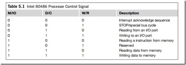
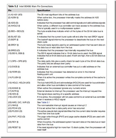
To allow for easy upgrades and to save space, the 80486 and Pentium processors are available in a pin- grid array (PGA) form. For all the Intel microprocessors, their PGA pin-out lists are provided in the corresponding Intel specifications. A 168-pin 80486 GX block is illustrated in Figure 5.1; it can be seen that the 80486 processor has a 32-bit address bus (A0-A31) and a 32-bit data bus (D0-D31). Table 5.1 defines how the 80486 control signals are interpreted. Table 5.2 lists the main input (I) and output (O) pins of Intel 80486 processor.
(6) Interrupt system
In the Intel microprocessors, the interrupt line types can be interrupt request pin (INTR), nonmaskable interrupt request pin (NMI), and system reset pin (RESET), all of which are high signals. The INTR pin is activated when an external device, such as a hard disk or a serial port, wishes to communicate with the processor. This interrupt is maskable can be ignored if necessary. The NMI pin is a non- maskable interrupt and so is always acted on. When it becomes active the processor calls the non- maskable interrupt service routine. The RESET pin signal causes a hardware reset and is normally activated when the processor is powered up.
Microprocessor interrupt operations
The interrupt I/O is a process of data transfer, whereby an external device or peripheral can inform the processor that it is ready for communication and it requests attention. The process is initiated by an external device and is asynchronous, meaning that it can be initiated at any time without reference to
the system clock. However, the response to an interrupt request is directed or controlled by the microprocessor. Unlike the polling technique, interrupt processing allows a program, or an external device, to interrupt the current task. An interrupt can be generated by hardware (hardware interrupt) or by software (software interrupt). At this point an interrupt service routine (ISR) is called. For a hardware interrupt, the ISR then communicates with the device and processes data, after which it returns to the original program. A software interrupt causes the program to interrupt its execution and go to an ISR. Software interrupts include the processor-generated interrupts that normally occur either when a program causes a certain type of error, or if it is being used in debug mode. In the latter case the program can be made to break from its execution when a breakpoint occurs. Software interrupts, in most cases, do not require the program to return when the ISR task is complete. Apart from this difference, both software and hardware interrupts use the same mechanisms, methodologies, and processes to handle interrupts.
Interrupt requests are classified as maskable interrupt and nonmaskable interrupt. The microprocessor can ignore or delay a maskable interrupt request if it is performing some critical task; however, it must respond to a nonmaskable interrupt immediately.
(1) Interrupt process
The operation of an interrupt depends upon the system mode in which when the interrupt occurs, either real mode or protection mode.
(1) The operation of a real mode interrupt
When the microprocessor completes executing the current instruction, it determines whether an interrupt is active by checking (1) instruction executions, (2) single step, (3) NMI pin, (4) coprocessor segment overrun, (5) INTR pin, and (6) INT instruction, in the order presented. If one or more of these interrupt conditions are present:
1. The contents of the flag register are pushed onto the stack.
2. Both the interrupt (IF) and trap (TF) flags are cleared. This disables the INTR pin and the trap or single-step feature.
3. The contents of the code segment register (CS) are pushed onto the stack.
4. The contents of the instruction pointer (IP) are pushed onto the stack.
5. The interrupt vector contents are fetched, and then placed into both IP and CS so that the next instruction executes the ISR addressed by the vector.
Whenever an interrupt is accepted, the microprocessor stacks the contents of the flag register, CS and IP; clears both IF and TF and then jumps to the procedure addressed by the interrupt vector. After the flags are pushed onto the stack, IF and TF are cleared. These flags are returned to the state prior to the interrupt when the IRET instruction is encountered at the end of the ISR. Therefore, if interrupts were enabled prior to the ISR, they are automatically re-enabled by the IRET instruction at the end of the interrupt service routine.
The return address (stored in CS and IP) is pushed onto the stack during the interrupt. Sometimes,
the return address points to the next instruction in the program, and sometimes it points to the instruction or point in the program where the interrupt occurred. Interrupt type numbers 0, 5, 6, 7, 8, 10, 11, 12, and 13 push a return address that points to the offending instruction, instead of to the next instruction in the program. This allows the ISR to retry the crashed instruction in certain error cases.
Some of the protected mode interrupts (type 8, 10, 11, 12, and 13) place an error code on the stack following the return address. This code identifies the selector that caused the interrupt. If no selector is involved, the error code is 0.
(2) The operation of a protected mode interrupt
In protected mode, interrupts have exactly the same assignments as in real mode, but the interrupt vector table is different. In place of interrupt vectors, protected mode uses a set of 256 interrupt descriptors that are stored in an interrupt descriptor table (IDT), normally 256 x 8 (2k) bytes long, with each descriptor containing 8 bytes. It is located at any memory location in the system by the IDT address register (IDTR). Each entry in the IDT contains the address of the ISR, in the form of a segment selector and a 32-bit offset address. It also contains the P bit (present) and DPL bits, which describe the privilege level of the interrupt.
Real mode interrupt vectors can be converted into protected mode interrupts by copying the interrupt procedure addresses from the interrupt vector table and converting them to 32-bit offset addresses that are stored in the interrupt descriptors. A single selector and segment descriptor can be placed in the global descriptor table that identifies the first 1M byte of memory as the interrupt segment.
Other than the IDT and interrupt descriptors, the protected mode interrupt functions like the real mode interrupt. They return from both interrupts by using the IRET or IRETD instruction. The only difference is that in protected mode the microprocessor accesses the IDT instead of the interrupt vector table.
(3) Interrupt flag bits
The interrupt flag (IF) and trap flag (TF) are both cleared after the contents of the flag register are stacked during an interrupt. When the IF bit is set, it allows the INTR pin to cause an interrupt; when the IF bit is cleared, it prevents the INTR pin from causing an interrupt. When IF ¼ 1, it causes a trap interrupt (interrupt type number 1) to occur after each instruction executes. This is why we often call trapping a single step. When TF ¼ 0, normal program execution occurs. The interrupt flag is set and cleared by the STI and CLI instructions, respectively. There are no special instructions that set or clear the trap flag.
(2) Interrupt vectors
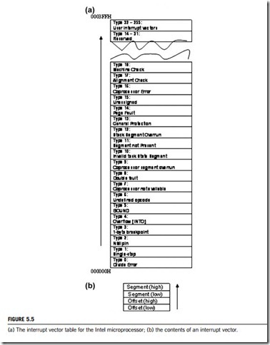
The interrupt vectors and vector table are crucial to the understanding of hardware and software interrupts. Interrupt vectors are addresses that inform the interrupt handler as to where to find the ISR (interrupt service routine, also called interrupt service procedure). All interrupts are assigned a number from 0 to 255, with each of these interrupts being associated with a specific interrupt vector.
The interrupt vector table is normally located in the first 1024 bytes of memory at addresses 000000H 0003FFH. It contains 256 different interrupt vectors. Each vector is 4 bytes long and contains the starting address of the ISR. This starting address consists of the segment and offset of the ISR. Figure 5.5 illustrates the interrupt vector table used for the Intel microprocessors. Remember that in order to install an interrupt vector (sometimes called a hook), the assembler must address absolute memory.
In an interrupt vector table, the first five interrupt vectors are identical in all Intel microprocessor family members, from the 8086 to the Pentium. Other interrupt vectors exist for the 80286 that are upward-compatible to 80386, 80486, and Pentium to Pentium 4, but not downward-compatible to the
(3) Interrupts service routine (ISR)
The interrupts of the entire Intel family of microprocessors include two hardware pins that request interrupts (INTR pin and NMI pin), and one hardware pin (INTA) that acknowledges the interrupt requested through INTR. In addition to these pins, the Intel microprocessor also has software interrupt instructions: INT, INTO, INT 3, and BOUND. Two flag bits, IF (interrupt flag) and TF (trap flag), are also used with the interrupt structure and with a special return instruction IRET (or IRETD in the 80386, 80486, or Pentium-Pentium 4).
(1) Software interrupts
Intel microprocessors provide five software interrupt instructions: BOUND, INTO, INT, INT 3, and IRET. Of these five instructions, INT and INT 3 are very similar, BOUND and INTO are conditional, and IRET is a special interrupt return instruction.
The INT n instruction calls the ISR that begins at the address represented by the vector number n. The only exception to this is the “INT 3” instruction, a 1-byte instruction, which is used as breakpoint- interrupt, because it is easy to insert a 1-byte instruction into a program. As mentioned previously, breakpoints are often used to debug faulty software.
The BOUND instruction, which has two operands, compares a register with two words of memory data. The INTO instruction checks the overflow flag (OF); If OF ¼ 1, the INTO instruction calls the ISR whose address is stored in interrupt vector type number 4. If OF ¼ 0, then the INTO instruction performs no operation and the next sequential instruction in the program executes.
The IRET instruction is a special return instruction used to return for both software and hardware interrupts. The IRET instruction is much like a “far RET” because it retrieves the return address from the stack. It is unlike the “near return” because it also retrieves a copy of the flag register. An IRET instruction removes six bytes from the stack: two for the IP, two for CS, and two for flags. In the 80386 to the Pentium 4, there is also an IRETD instruction, because these microprocessors can push the EFLAG register (32 bit) on the stack, as well as the 32-bit EIP in protected mode. If operated in the real mode, we use the IRET instruction with the 80386 to Pentium 4 microprocessors.
(2) Hardware interrupts
The microprocessor has two hardware inputs; nonmaskable interrupt (NMI) and interrupt request (INTR). Whenever the NMI input is activated, a type 2 interrupt occurs because NMI is internally decoded. The INTR input must be externally decoded to select a vector. Any interrupt vector can be chosen for the INTR pin, but we usually use an interrupt type number between 20H and FFH. Intel has reserved interrupts 00H through 1FH for internal and future expansion. The INTA signal is also an interrupt pin on the microprocessor, but it is an output that is used in response to the INTR input to apply a vector-type number to the data bus connections D7 D0.
The NMI is an edge-triggered input that requests an interrupt on the positive edge (0-to-1 tran- sition). After a positive edge, the NMI pin must remain logic 1 until it is recognized by the micro- processor. The NMI input is often used for parity errors and other major system faults, such as power failure. Power failures are easily detected by monitoring the AC (alternating current) power line and causing an NMI interrupt whenever AC power drops out.
The interrupt request input (INTR) is level-sensitive, which means that it must be held at logic 1 level until it is recognized. The INTR pin is set by an external event and cleared inside the ISR. This input is automatically disabled once it is accepted by the microprocessor and reenabled by the IRET instruction at the end of the ISR. The microprocessor responds to the INTR input by pulsing the INTA output in anticipation of receiving an interrupt vector-type number on data bus connection D7 D0. There are two INTA pulses generated by the system that are used to insert the vector-type number on the data bus.
Microprocessor unit input/output rationale
The I/O devices can be interfaced with a microprocessor using two techniques: isolated I/O (also called peripheral-mapped I/O) and memory-mapped I/O. The process of data transfer in both is identical. Each device is assigned a binary address, called a device address or port number, through its interface circuit. When the microprocessor executes a data transfer instruction for an I/O device, it places the appropriate address on the address bus, sends the control signals, enables the interfacing device, and then transfers data. The interface device is like a gate for data bits, which is opened by the micro- processor whenever it intends to transfer data.
(1) Basic input/output techniques
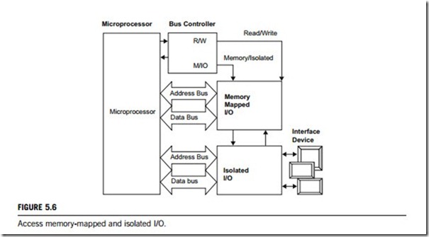
As previously mentioned, there are two main methods of communicating with external equipment either the equipment is mapped into the physical memory and given a real address on the address bus of the microprocessor (memory-mapped I/O), or it is mapped into a special area of input/output memory (isolated I/O). Devices mapped into memory are accessed by reading or writing to its physical address. Isolated I/O provides ports that are gateways between the interface device and the processor. They are isolated from the system using a buffering system, and are accessed by four machine code instructions: IN, INS, OUT, OUTS. The IN (INS) instruction inputs a byte, or a word, and the OUT (OUTS) instruction outputs a byte, or a word. A high-level compiler interprets the equivalent high-level functions and produces machine code that uses these instructions.
Figure 5.6 shows the two methods. This figure also tells us that devices are not directly connected to the address and data bus because they may use part of the memory that a program uses or they could cause a hardware fault. This device interprets the microprocessor signals and generates the required memory signals. Two main output lines differentiate between a read and a write operation (R/W) and between direct and isolated memory access (M/IO). The R/W line is low when data are being written to memory and high when data are being read. When M/IO is high, direct memory access is selected, and when low, the isolated memory is selected.
(1) Isolated I/O
The most common I/O transfer technique used in the Intel microprocessor-based system is isolated I/O. The term “isolated” describes how the I/O locations are isolated from the memory system in a separate I/O address space. The addresses for isolated I/O devices, called ports, are separate from the memory, hence the user can expand the memory to its full size without using any of the memory space reserved for I/O devices. A disadvantage of isolated I/O is that the data transferred between I/O and the microprocessor must be accessed by the IN, INS, OUT, and OUTS instructions. Separate control signals for the I/O space are developed (using M/IO and R/W), which indicate an I/O read (IORC) or an I/O write (IOWC) operation. These signals indicate that an I/O port address, which appears on the
address bus, is used to select the I/O device. In the personal computer, isolated I/O ports are used for controlling peripheral devices such as direct memory access (DMA) controller, NMI reset, game I/O adaptor, floppy disk controller, second serial port (COM2), and primary serial port (COM1). An 8-bit port address is used to access devices located on the system board, such as the timer and keyboard interface, while a 16-bit port is used to access serial and parallel ports as well as video and disk drive system.
(2) Memory-mapped I/O
Interface devices can map directly onto the system address and data bus. Unlike isolated I/O, memory-mapped I/O does not use the IN, INS, OUT, or OUTS instructions. Instead, it uses any instruction that transfers data between the microprocessor and memory. A memory-mapped I/O device is treated as a memory location in the memory map, the main advantage of this being that any memory transfer instruction can be used to access the I/O device. The main disadvantage is that a portion of the memory system is used as the I/O map, which reduces the amount of usable memory available for applications.
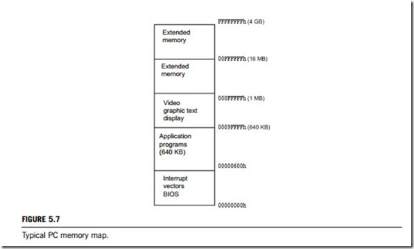
In a PC-compatible system the address bus is 20 bits wide, from address 00000h to FFFFFh (1MB).
Figure 5.7 gives a typical memory allocation in PC.
(2) Basic input/output interfaces
The basic input device is a set of three-state buffers, and the basic output device is a set of data latches. The term IN refers to moving data from the I/O device into the microprocessor, and the term OUT refers to moving data out of the microprocessor to the I/O device.
Many I/O devices accept or release information at a much slower rate than the microprocessor. Another method of I/O control, called handshaking or polling, synchronizes the I/O device with the
microprocessor. An example of a device that requires handshaking is a parallel printer that prints 100 characters per second (CPS). It is obvious that the microprocessor can send more than 100 CPS to the printer, so a handshaking must be used to slow the microprocessor down to match the speed of printer.
(1) The basic input interface
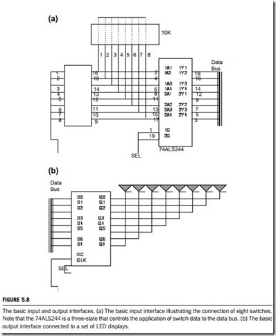
Three-state buffers 74ALS244 are used to construct the 8-bit input port depicted in Figure 5.8(a). The external TTL data (simple toggle switches in this example) are connected to the inputs of the buffers. The outputs of the buffers connect to the data bus. The exact data bus connections depend on the version of the microprocessor. For example, the 8088 has data bus connections D7 D0, the 80486 has D31 D0, and the Pentium to Pentium 4 have D63 D0. The circuit of Figure 5.8(a) allows the microprocessor to read the contents of the eight switches that connect to any 8-bit section of the data bus when the select signal SEL becomes logic 0. Thus, whenever the IN instruction executes, the contents of the switches are copied into the AL register.
When the microprocessor executes an IN instruction, the I/O port address is decoded to generate the logic 0 on SEL. A 0 placed on the output control inputs (1G and 2G) of the 74ALS244 buffer causes the data input connections (A) to be connected to the data input (Y) connections. If a logic 1 is placed on the output control inputs of the 74ALS244 buffer, the device enters the three-state high- impedance mode that effectively disconnects the switches from the data bus.
The basic input circuit is not optional and must appear any time that input data are interfaced to the microprocessor. Sometimes it appears as a discrete part of the circuit, as shown in Figure 5.8(a); sometimes it is built into a programmable I/O device.
It is possible to interface 16- or 32-bit data to various versions of the microprocessor, but this is not nearly as common as using 8-bit data. To interface 16 bits of data, the circuit in Figure 5.8(a) is doubled to include two 74ALS244 buffers that connect 16 bits of input data to the 16-bit data bus. To interface 32 bits of data, the circuit is expanded by a factor of 4.
(2) The basic output interface
The basic output interface receives data from the microprocessor and must usually hold them for some external device. Its latches or flip-flops, like the buffers found in the input device, are often built into the I/O device.
Figure 5.8(b) shows how eight simple light-emitting diodes (LEDs) connect to the microprocessor through a set of eight data latches. The latch stores the number that is output by the microprocessor vice the data bus so that the LED can be lit with any 8-bit binary number. Latches are needed to hold the data, because when the microprocessor executes an OUT instruction, the data are present on the data bus for less than 1.0 m s. Without a latch, the viewer would never see the LED illuminate.
When the OUT instruction executes, the data from AL, AX, or EAX are transferred to the latch via the data bus. Here, the D inputs of a 74ALS374 octal latch are connected to the data bus to capture the output data, and the Q outputs of the latch are attached to the LED. When a Q becomes a logic 0, the LED lights. Each time that the OUT instruction executes, the SEL signal to the latch activates, capturing the data output to the latch from any 8-bit section of the data bus. The data are held until the next OUT instruction executes. Thus, whenever the output instruction is executed in this circuit, the data from the AL register appear on the LED.
Microprocessor unit bus system operations
This subsection uses the peripheral component interconnect (PCI) bus to introduce the microprocessor unit bus system operations. The PCI bus has been developed by Intel for its Pentium processors. This technique can be populated with adaptors requiring fast accesses to each other and/or system memory, and that can be accessed by the processor at speeds approaching that of the processor’s full native bus. A PCI physical device package may take the form of a component integrated onto the system board, or may be implemented on a PCI add-in card. Each PCI package (referred to in the specification as a device) may incorporate from one to eight separate functions. A function is a logical device, which contains its own, individually addressable configuration space, 64 double words in size. Its configu- ration registers are implemented in this space. Using these registers, the configuration software can automatically detect the presence of a function, determine its resource requirements including memory space, I/O space, interrupt lines, etc., and can then assign resources to the function that are guaranteed not to conflict with the resources assigned to other devices.
(1) Bus operations
The PCI bus operates in multiplexing mode (also called normal mode) and/or in burst mode. In the former, the address and data lines are used alternatly. First, the address is sent, followed by a data read or write. Unfortunately, this mode requires two or three clock cycles for a single transfer of an address followed by a read or write cycle. The multiplex mode obviously slows down the maximum transfer rate.
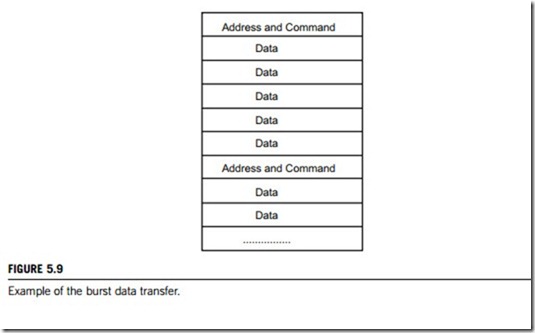
Additionally, a PCI bus can be operated in burst mode. A burst transfer consists of a single address phase followed by two or more data phases. In this mode, the bus master only has to arbitrate for bus ownership once. The start addresses and transaction type are issued during the address phase. All devices on the bus latch the address and transaction type and decode them to determine which the target device is. The target device latches the start address into an address counter and is responsible for incrementing the address from data phase to data phase. Figure 5.9 shows an example of burst data transfer.
There are two participants in every PCI burst transfer; the initiator and the target. The initiator, or bus master, is the device that initiates a transfer. The target is the device currently addressed by the initiator for the purpose of performing a data transfer. PCI initiator and target devices are commonly referred to as PCI-compliant agents in the specifications. It should be noted that a PCI target may be designed such that it can only handle single data phase transactions. When a bus master attempts to perform a burst transaction, the target forces the master to terminate the transaction at the completion of the first data phase. The master must rearbitrate for the bus to attempt resumption of the burst when the next data phase completes. In each burst transfer; (1) the address and the transfer type are output during the address phase; (2) a data object may then be transferred during each subsequent data phase.
Assuming that neither the initiator nor the target device inserts wait states in each data phase, a data
object may be transferred on the rising edge of each PCI clock cycle. At a PCI bus clock frequency of 33 MHz, a transfer rate of 132 MB/s may be achieved. A transfer rate of 264 MB/s may be achieved in a 64-bit implementation when performing 64-bit transfers during each data phase.
(1) Address phase
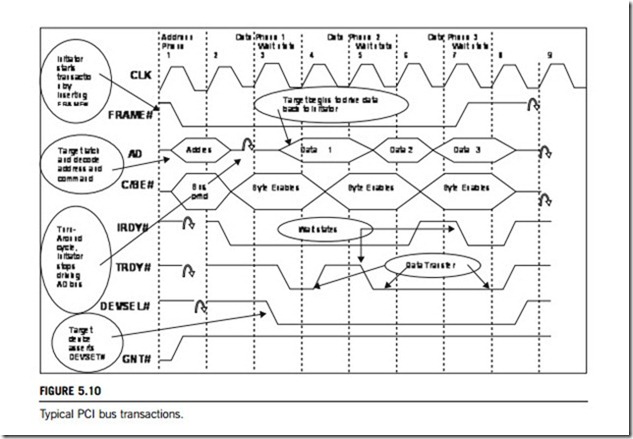
Refer to Figure 5.10. Every PCI transaction (with the exception of a transaction using 64-bit addressing) starts off with an address phase one PCI clock period in duration. During the address phase, the initiator identifies the target device and the type of transaction (also referred to as command type). The target device is identified by driving a start address within its assigned range onto the PCI
address and data bus. At the same time, the initiator identifies the type of transaction by driving the command type onto the 4-bit-wide PCI Command/Byte Enable bus. The initiator also asserts the FRAME# signal to indicate the presence of a valid start address or transaction type on the bus. Since the initiator only presents the start address and command for one PCI clock cycle, it is the respon- sibility of every PCI target device to latch the address and command on the next rising edge of the clock so that it may subsequently be decoded.
By decoding the address latched from the address bus, and the command type latched from the Command/Byte Enable bus, a target device can determine whether it is being addressed or not, and the type of transaction that is in progress. It is important to note that the initiator only supplies a start address to the target during the address phase. Upon completion of the address phase, the address or data bus becomes the data bus for the duration of the transaction and is used to transfer data in each of the data phases. It is the responsibility of the target to latch the start address, and to autoincrement it to point to the next group of locations during each subsequent data transfers.
(2) Data phase
Refer to Figure 5.10. The data phase of a transaction is the period during which a data object is transferred between the initiator and the target. The number of data bytes to be transferred during a data phase is determined by the number of Command/Byte Enable signals that are asserted by the initiator during the data phase. Each data phase is at least one PCI clock period in duration. Both the initiator and the target must indicate that they are ready to complete a data phase, or else it is extended by a wait state that is one PCI CLK period in duration. The PCI bus defines ready signal lines to be used by both the initiator (IRDY#) and the target (TRDY#) for this purpose. The initiator does not issue a transfer count to the target. Rather, in each data phase it indicates whether it is ready to transfer the current data item and, if it is, whether it is the final data item. FRAME# is inserted at the start of the address phase and remains inserted until the initiator is ready (inserts IRDY#) to complete the final data phase. When the target samples IRDY# are inserted and FRAME# are not inserted, it realizes that this is the final data phase.
Refer to Figure 5.10. The initiator indicates that the last data transfer (of a burst transfer) is in progress by uninserting FRAME# and inserting IRDY#. When the last data transfer has been completed, the initiator returns the PCI bus to the idle state by uninserting its ready line (IRDY#). If another bus master had previously been granted ownership of the bus by the PCI bus arbiter and was waiting for the current initiator to surrender the bus, it can detect that the bus has returned to the idle state by detecting FRAME# and IRDY# are both uninserted on the same rising edge of the PCI clock.
(2) Bus system arbitration
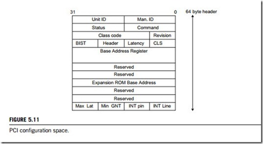
Bus masters are devices on a PCI bus that are allowed to take control of that bus. This is done by a component named a bus arbiter, which usually integrated into the PCI chipset. Specifically, it is typically integrated into the host/PCI or the PCI/expansion bus bridge chip. Each master device is physically connected to the arbiter via a separate pair of lines, with each of them being used as REQ# (request) signal or GNT# (grant) signal, respectively. Ideally, the bus arbiter should be programmable by the system. If it is, the startup configuration software can determine the priority to be assigned to each member by reading from the maximum latency (Max Lat) configuration register associated with each bus master (see Figure 5.11). The bus designer hardwires this register to indicate, in increments of 250 ns, how quickly the master requires access to the bus in order to achieve adequate performance.
At a given instant in time, one or more PCI bus master devices may require use of the PCI bus to perform a data transfer to another PCI device. Each requesting master asserts its REQ# output to confirm to the bus arbiter its pending request for the use of the bus. In order to grant the PCI bus to a bus master, the arbiter asserts the device’s respective GNT# signal. This grants the bus to a bus master for one transaction, as shown in Figure 5.10. If a master generates a request, it is subsequently granted the bus and does not then initiate a transaction by asserting FRAME# signal within 16 PCI clocks after the bus goes idle, the arbiter may then assume that this bus master is malfunctioning. The action taken by the arbiter would then depend upon the system design. If a bus master has another transaction to perform immediately after the one it just initiated, it should keep its REQ# line asserted when it asserts the FRAME# signal to begin the current transaction. This informs the arbiter of its desire to maintain ownership of the bus after completion of the current transaction. In the event that ownership is not maintained, the master should keep its REQ# line asserted until it is successful in acquiring bus ownership again.
At a given instant in time, only one bus master may use the bus. This means that no more than one GNT# line will be asserted by the arbiter during any PCI clock cycle. On the other hand, a master must only assert its REQ# output to signal a current need for the bus. This means that a master must not use its REQ# line to “park” the bus on itself. If a system designer implements a bus parking scheme, the bus arbiter design should indicate a default bus owner by asserting the device’s GNT# signal when no request from any bus masters are currently pending. In this manner, signal REQ# from the default master is granted immediately once no other bus masters require the use of the PCI bus.
The PCI specification does not define the scheme to be used by the PCI bus arbiter to decide the winner of any competition for bus ownership. The arbiter may utilize any scheme, such as one based on fixed, or rotational priority, or a combination of these two, to avoid deadlocks. However, the central arbiter is required to implement a fairness algorithm to avoid deadlocks. Fairness means that each potential bus master must be granted access to the bus independently of other requests. Fairness is defined as a policy that ensures that high-priority masters will not dominate the bus to the exclusion of lower-priority masters when they are continually requesting the bus. However, this does not mean that all agents are required to have equal access to the bus. By requiring a fairness algorithm there are no special conditions to handle when the signal LOCK# is active (assuming a resource lock) or when cacheable memory is located on the PCI. A system that uses a fairness algorithm is still considered fair if it implements a complete bus lock instead of a resource lock. However, the arbiter must advance to a new agent if the initial transaction attempting to establish a lock is terminated with retry.
(3) Interrupt routing
The host/PCI bus bridge will transfer the interrupt acknowledgment cycle from the processor to the PCI bus, which requires that the microprocessor chipset has an interrupt routing functionality. This router for the interrupt routing could be implemented using an Intel APIC I/O module, as given in Figure 5.3(a). This module can be programmed to assign a separate interrupt vector (interrupt table entry number) for each of the PCI interrupt request lines. It can also be programmed so that it realizes that one of its inputs is connected to an Intel programmable interrupt controller. If a system does not have this kind of controller, the microprocessor chipset should incorporate a software programmable interrupt routine device. In this case, the startup configuration software of the microprocessor attempts to program the router to distribute the PCI interrupt in an optimal fashion.
182 CHAPTER 5 Microprocessors
Whenever any of the PCI interrupt request lines is asserted, the APIC I/O module supplies the vector (see Figure 5.5 for an interrupt vector table) associated with that input to the processor‘s embedded local APIC I/O module. Whenever this programmable interrupt controller generates a request, the APIC I/O informs the processor that it must poll this programmable interrupt controller to get this vector. In response, the Intel processor can generate two back-to-back Interrupt Ac- knowledge transactions. The first Interrupt Acknowledge forces this programmable interrupt con- troller to prioritize the interrupts pending, while the second Interrupt Acknowledge requests that the interrupt controller send the vector to the processor. For a detailed discussion of APIC operation, refer to the MindShare book entitled Pentium Processor System Architecture (published by Addison- Wesley). For a detailed description of the Programmable Interrupt Controller chipset, refer to section
6.3 of this textbook.
Figure 5.10 can also be used to explain an interrupt acknowledgment cycle on the PCI bus, where a single byte enable is asserted. The PCI bus performs only one interrupt acknowledgment cycle per interrupt. Only one device may respond to the interrupt acknowledgment; that device must assert DEVSEL#, indicating that it is claiming the interrupt acknowledgment. The sequence is as follows:
1. During the address phase, the AD signals do not contain a valid address; they must be driven with stable data so that parity can be checked. The C/BE# signals contain the interrupt acknowledge command code (not shown).
2. IRDY# and the BE#s are driven by the host/PCI bus bridge to indicate that the bridge (master) is ready for response.
3. The target will drive DEVSEL# and TRDY# along with the vector on the data bus (not shown).
(4) Configuration registers
Each PCI device has 256 bytes of configuration data, which is arranged as 64 registers of 32 bits. It contains a 64-byte predefined header followed by an extra 192 bytes which contain extra configuration data. Figure 5.11 shows the arrangement of the header. The definitions of the fields in this header are as follows:
1. Unit ID and Man. ID. A Unit ID of FFFFh defines that there is no unit installed, while any other address defines its ID. The PCI SIG, which is the governing body for the PCI specification, allocates a Man. ID. This ID is normally shown at BIOS start-up.
2. Status and command.
3. Class code and revision. The class code defines the PCI device type. It splits into two 8-bit values with a further 8-bit value that defines the programming interface for the unit. The first defines the unit classification, followed by a subcode which defines the actual type.
(1) BIST, header, latency, CLS
The built-in-self test (BIST) is an 8-bit field, where the most significant bit defines whether the device can carry out a BIST, the next bit defines whether a BIST is to be performed (a 1 in this position indicates that it should be performed), and bits 3 0 define the status code after the BIST has been performed (a value of zero indicates no error). The header field defines the layout of the 48 bytes after the standard 16-byte header. The most significant bit of the header field defines whether the device is a multifunction device or not. A1 defines a multifunction unit. The cache line size (CLS) field defines the size of the cache in units of 32 bytes. Latency indicates the length of time for a PCI bus operation, where the amount of time is the latency þ 8 PCI clock cycles.
(2) Base address register
This area of memory allows the device to be programmed with an I/O or memory address area. It can contain a number of 32- or 64-bit addresses. The format of a memory address is (i) Bit 64-4: base address; (ii) Bit 3: PRF. Prefetching, 0 identifies not possible, 1 identifies possible; (iii) Bit 2, 1: Type. 00, any 32-bit address; 01, less than 1 MB; 10, any 64-bit address; and 11, reserved; (iv) Bit 0: 0. Always set a 0 for a memory address. For an I/O address space it is defined as: (i) Bit 31-2: base address; (ii) Bit 1, 0: 01. Always set to a 01 for an I/O address.
(3) Expansion ROM base address
This allows a ROM expansion to be placed at any position in the 32-bit memory address area.
(4) Max Lat, Min GNT, INT-pin, INT-line
The Min GNT and Max Lat registers are read-only registers that define minimum and maximum latency values. The INT-line field is a 4-bit field that defines the interrupt line used (IRQ0 IRQ15). A value of 0 corresponds to IRQ0 and a value of 15 corresponds to IRQ15. The PCI bridge can then redirect this interrupt to the correct IRQ line. The 4-bit INT pin defines the interrupt line that the device is using. A value of 0 defines no interrupt line, 1 defines INTA, 2 defines INTB, and so on.
