Objectives
After studying this unit, the student will be able to:
• Discuss similarities between digital logic circuits and relay logic circuits
• Discuss different types of digital logic circuits
• Recognize gate symbols used for computer logic circuits
• Recognize gate symbols used for NEMA logic circuits Complete a truth table for the basic gates
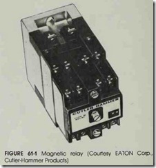
The electrician in today’s industry must be familiar with solid-state digital logic circuits. Dig ital, of course, means a device that has ·only two states, on or off. Most electricians have been using digital logic for many years without realizing it. Magnetic relays, for instance, are digital devices. Relays are generally considered to be single-input, multi-output devices. The coil is the input and the contacts are the output. A relay has only one coil, but it may have a large number of contacts, figure 61-1.
Although relays are digital devices, the term “digital logic” has come to mean circuits that use solid-state control devices known as gates. There are five basic types of gates: the AND, OR, NOR, NAND, and INVERTER. Each of these gates will be covered later in this text.
There are also different types of logic. For in stance, one of the earliest types of logic to appear was RTL which stands for resistor-transistor logic. This was followed by DTL which stands for diode transistor logic, and TTL which stands for transistor transistor logic. RTL and DTL are not used much anymore, but TTL is still used to a fairly large extent. TTL can be identified because it operates on 5 volts.
Another type of logic frequently used in in dustry is HTL which stands for high-transit logic. HTL is used because it does a better job of ignor ing the voltage spikes and drops caused by the
starting and stopping of inductive devices such as motors. HTL generally operates on 15 volts.
Another type of logic that has become very popular is CMOS, which has very high input impedance. CMOS comes from COSMOS which means complementary-symmetry metal-oxide-semicon ductor. The advantage of CMOS logic is that it re quires very little power to operate, but there are also some disadvantages. One disadvantage is that CMOS logic is so sensitive to voltage that the static charge of a person’s body can sometimes de stroy an IC just by touching it. People that work with CMOS logic often use a ground strap which straps around the wrist like a bracelet. This strap is used to prevent a static charge from building up on the body.
Another characteristic of CMOS logic is that unused inputs cannot be left in an indeterminate state. Unused inputs must be connected to either a high state or a low state.
THE AND GATE
While magnetic relays are single-input, multi output devices, gate circuits are multi-input, sin gle-output devices. For instance, an AND gate may have several inputs, but only one output. Fig ure 61-2 shows the USASI symbol for an AND gate with three inputs, labeled A, B, and C, and one output, labeled Y.
USASI symbols are more commonly referred
to as computer logic symbols. Unfortunately for industrial electricians, there is another system known as NEMA logic which uses a completel y different set of symbols. The NEMA symbol for a three-input AND gate is shown in figure 61-3.
Although both symbols mean the same thing, they are drawn differently. Electricians working in industry must learn both sets of symbols because both types of symbols are used. Regardless of which type of symbol is used, the AND gate op erates the same way. An AND gate must have all of its inputs high in order to get an output. If it is assumed that TTL logic is being used, a high level
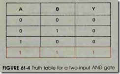
is considered to be + 5 volts and a low level is considered to be 0 volts. Figure 61-4 shows the truth table for a two-input AND gate .
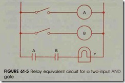
The truth table is used to illustrate the state of a gate’s output with different conditions of in put. The number one represents a high state and zero represents a low state. Notice in figure 61-4 that the output of the AND gate is high only when both of its inputs are high. The operation of the AND gate is very similar to that of the simple re lay circuit shown in figure 61-5.
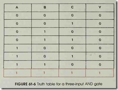
If a lamp is used to indicate the output of the AND gate, both relay coils A and B must be en ergized before there can be an output. Figure 61-6 shows the truth table for a three-input AND gate. Notice that there is still only one condition that permits a high output for the gate, and that condition is when all inputs are high or at logic level one.
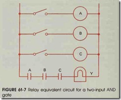
When using an AND gate, any zero input = a zero output. An equivalent relay circuit for a three-input AND gate is shown in figure 61-7.
THE OR GATE
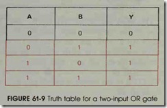
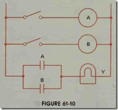
The computer logic symbol and the NEMA logic symbol for the OR gate are shown in figure 61-8. The OR gate has a high output when either or both of its inputs are high. Refer to the truth table shown in figure 61-9. An easy way to remem ber how an 0R gate functions is to say that any one input = a one output. An equivalent relay circuit for the OR gate is shown in figure 61-10. Notice in this circuit that if either or both of the relays are energized, there will be an output at Y.
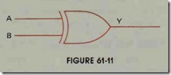
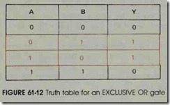
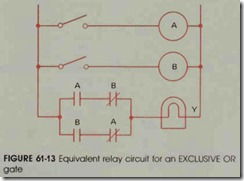
Another gate which is very similar to the OR gate is known as an EXCLUSIVE OR gate. The symbol for an EXCLUSIVE OR gate is shown in figure 61-11. The EXCLUSIVE OR gate has a high output when either, but not both, of its in puts are high. Refer to the truth table shown in figure 61-12. An equivalent relay circuit for the EXCLUSIVE OR gate is shown in figure 61-13. Notice that if both relays are energized or de-en ergized at the same time, there is no output.
THE INVERTER
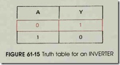
The simplest of all the gates is the IN VERTER . The INVERTER has one input and one output. As its name implies, the output is in verted, or the opposite of the input. For example, if the input is high, the output is low, or if the input is low, the output is high. Figure 61-14 shows the computer logic and NEMA symbols for an IN VERTER.
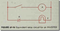
In computer logic, a circle drawn on a gate means to invert. Since the “0” appears on the out put end of the gate, it means the output is in verted. In NEMA logic an X is used to show that a gate is inverted. The truth table for an IN VERTER is shown in figure 61-15. The truth ta ble clearly shows that the output of the IN VERTER is the opposite of the input. Figure 61- 16 shows an equivalent relay circuit for the IN VERTER.
THE NOR GATE
The NOR gate is the “NOT OR” gate. Re ferring to the computer logic and NEMA logic symbols for a NOR gate in figure 61-17, notice that the symbol for the NOR gate is the same as the symbol for the OR gate with an inverted out put. A NOR gate can be made by connecting an INVERTER to the output of an OR gate as shown in figure 61-18.
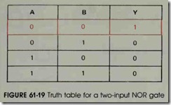
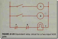
The truth table shown in figure 61-19 shows that the output of a NOR gate is zero, or low, when any input is high. Therefore, it could be said that any one input = a zero output for the NOR gate. An equivalent relay circuit for the NOR gate is shown in figure 61-20. Notice in figure 61-20 that if either relay A or B is energized, there is no output at Y.
THE NAND GATE
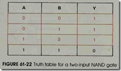
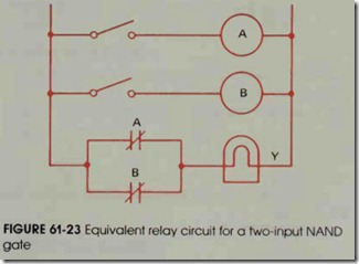
The NAND gate is the “NOT AND” gate. Figure 61-21 shows the computer logic symbol and the NEMA logic symbol for the NAND gate. Notice that these symbols are the same as the sym bols for the AND gate with inverted outputs. If any input of a NAND gate is low, the output is high. Refer to the truth table in figure 61-22. No tice that the truth table clearly indicates that any zero input = a one output. Figure 61-23 shows an equivalent relay circuit for the NAND gate. If eigher relay A or relay B is de-energized, there is an output at Y.
The NAND gate is often referred to as the basix gate because it can be used to make any of the other gates. For instance, figure 61-24 shows the NAND gate connected to make an IN VERTER. If a NAND gate is used as an IN VERTER and is connected to the output of an other NAND gate, it will become an AND gate as shown in figure 61-25. When two NAND gates are connected as INVERTERS, and these IN VERTERS are connected to the inputs of another NAND gate, an OR gate is formed, figure 61-26. If an INVERTER is added to the output of the OR gate shown in figure 61-26, a NOR gate is formed, figure 61-27.
INTEGRATED CIRCUITS
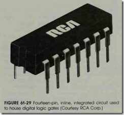
Digital logic gates are generally housed in fourteen-pin, IC packages. One of the old reliable types of TTL logic which is frequently used is the 7400 family of devices. For instance, a 7400 IC is a quad, two-input, positive NAND gate. The word quad means that there are four NAND gates contained in the package. Each NAND gate has two inputs, and positive means that a level one is considered to be a positive voltage.
There can, however, be a difference in the way ICs are connected. A 7400 (J or N) IC has a different pin connection than a 7400 (W) package. In figure 61-28, both ICs contain four two-input NAND gates, but the pin connections are differ ent. For this reason, it is necessary to use a con nection diagram when connecting or testing inte grated circuits. A fourteen-pin IC is shown in figure 61-29.
TESTING INTEGRATED CIRCUITS
Integrated circuits cannot be tested with a volt-ohm-milliammeter. Most ICs must be tested by connecting power to them and then testing the inputs and outputs with special test equipment. Most industrial equipment is designed with differ ent sections of the control system built in modular form. The electrician determines which section of the circuit is not operating and replaces that mod ule. The defective module is then sent to the elec tronics department or to a compan y outside of the plant for repair.
REVIEW QUESTIONS
1. What type of digital logic operates on 5 volts?
2. What precautions must be taken when connecting CMOS logic?
3. What do the letters COSMOS stand for?
4. When using a two-input AND gate, what conditions of input must be met to have an output?
5. When using a two-input OR gate, what conditions of input must be met to have an output?
6. Explain the difference between an OR gate and an EXCLUSIVE OR gate.
7. When using a two-input NOR gate, what condition of input must be met to have an output?
8. When using a two-input NAND gate, what condition of input must be met to have an output?
9. If an INVERTER is connected to the output of a NAND gate, what logic gate is formed?
10. If an INVERTER is connected to the output of an OR gate, what gate is formed?
11. What symbol is used to represent “invert” when computer logic symbols are used?
12. What symbol is used to represent “invert” when NEMA logic symbols are used?
