Power BJTs vs Power MOSFETs as Amplifier Output Devices
Some rivalry appears to have arisen between audio amplifier designers over the relative merits of power BJTs, as compared with power MOSFETs. Predictably, this is a mixture of advantages and drawbacks. Because of the much more elaborate construction of the MOSFET, in which a multiplicity of parallel connected conducting channels is fabricated to reduce the conducting “on” resistance, the chip size is larger and the device is several times more expensive both to produce and to buy. The excellent HF characteristics of the MOSFET, especially the N-channel V and U MOS types, can lead to unexpected forms
of VHF instability, which can, in the hands of an unwary amplifier designer, lead to the rapid destruction of the output devices. However, this excellent HF performance, when handled properly, makes it much easier to design power amplifiers with good gain and phase margins in the feedback loop, where overall NFB is employed. In contrast, the relatively sluggish and complex characteristics of the junction power transistor can lead to difficulties in the design of feedback amplifiers with good stability margins.
Also, as has been noted, the power MOSFET is intrinsically free from the problem of secondary breakdown, and an amplifier based on these does not need the protective circuitry that is essential in amplifiers with BJT output devices if failure is to be avoided when they are used at high power levels with very low impedance or reactive loads.
The problem here is that the protective circuitry may cut in during high-frequency signal level peaks during the normal use of the amplifier, which can lead to audible clipping. (Incidentally, the proponents of thermionic valve-based audio amplifiers have claimed that the superior audible qualities of these, by comparison with transistor-based designs, are due to the absence of any overload protection circuitry that could cause premature clipping and to their generally more graceful behavior under sporadic overload conditions).
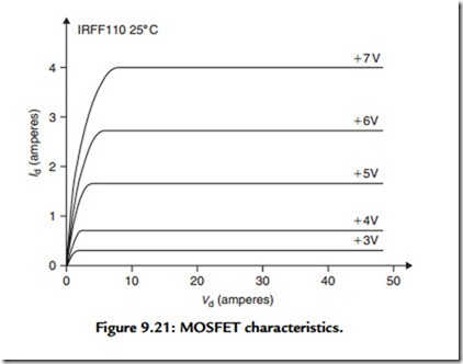
A further benefit enjoyed by the MOSFET is that it is a majority carrier device, which means that it is free from the hole-storage effects that can impair the performance of power junction transistors and make them sluggish in their turn-off characteristics at high collector current levels. However, on the debit side, the slope of the Vg/Id curve of the MOSFET is less steep than that of the Vb/Ic curve of the BJT, which means that the output impedance of power MOSFETs used as source followers is higher than that of an equivalent power BJT used as an emitter follower. Other things being equal, a greater amount of overall negative feedback (i.e., a higher loop gain) must therefore be used to achieve the same low amplifier output impedance with a power MOSFET design than would be needed with a power BJT one. If a pair of push–pull output source/emitter followers is to be used in a class AB output stage, more forward bias will be needed with the MOSFET than with the BJT to achieve the optimum level of quiescent operational current, and the discontinuity in the push–pull transfer characteristic will be larger in size, although likely to introduce, in the amplifier output signal, lower rather than higher order crossover harmonics.
