Discrete Semiconductor Failure Modes
Failures of semiconductor devices in storage, or dormant applications, are the result of latent manufacturing defects that were not detected during device screening tests. For discrete semiconductors, such as transistors, a large percentage of failures are the result of die and wire bonding defects and contamination. A common failure mode of spring loaded diodes is the contact material losing its compression strength, or slipping off the die, resulting in an open circuit.
Failure mechanisms can be grouped into three categories:
-
Those independent of environment (oxide defects, diffusion defects).
-
Failure mechanisms that are time and environment dependent (metal migration, corrosion, intermetallic compound formulations, such as caused by dissimilar metal use).
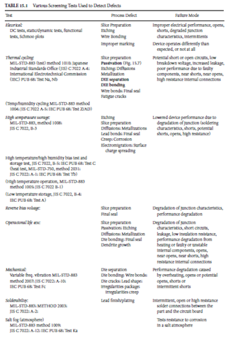
Table 15.1 and Sec. 15.6 discusses the various screening tests to induce failures prior to components being incorporated in assemblies.
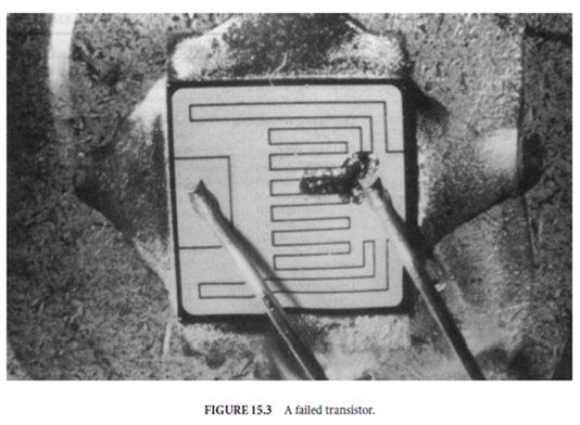
Common failure modes of discrete semiconductors are zener diode: 50% short, 50% open; junction diode: 60–70% high reverse, 20–25% open, 10–15% short; silicon controlled rectifier (SCR): 2% open, 98% short; and transistor: 20% high leakage, 20% low gain, 30% open circuit, 30% short circuit (Fig. 15.3).
-
General purpose diode: 49% short, 36% open, 15% parameter change
-
Diode rectifier: 51% short, 29% open, 20% parameter change
-
Small signal diode: 18% short, 24% open, 58% parameter change
-
Microwave diode: 50% open, 23% parameter change (drift), 10% short, 17% intermittent
-
Zener diode reference: 68% parameter change (drift), 17% open, 13% shorted, 2% intermittent
-
Zener diode regulator: 45% open, 35% parameter change (drift), 20% shorted
-
Optoelectronic LED: 70% open, 30% short
-
Optoelectronic sensor: 50% short, 50% open
-
Thyristor: 45% failed off, 40% short, 10% open, 5% failed on
-
Triac: 90% failed off, 10% failed on
Further breakdown on transistor failure modes by the Reliability Analysis Center (RAC) are
-
Bipolar transistor: 73% shorted, 27% open
(Note these new data contrast with that published in January 1976 by the U.S. Army Material Command (AMCP-706-196), which had 59% high collector to base leakage current, 37% low collector to emitter breakdown (Bvceo), and 4% open circuited).
-
Field effect transistor (FET): 51% shorted, 22% low output, 17% parameter change, 5% open, 5% output high
-
GaAs FET transistor: 61% open, 26% shorted, 13% parameter change
-
Radio frequency (RF) transistor: 50% parameter change, 40% shorted, 10% open
Integrated Circuit Failure Modes
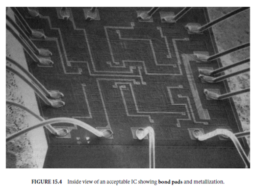
Most IC failures, as for semiconductors, are related to manufacturing defects (Fig. 15.4 is the inside view of a typical acceptable IC). A breakdown of typical IC failure mechanisms is 40.7% wire bond interconnects, 23.4% misapplication/misuse, 4.2% masking/etching defect, 3.3% die mechanical damage, 1.4% cracked die, 0.9% die metallization corrosion, 0.9% die contamination, and 24.8% other causes.
These mechamisms result in the following typical failure modes:
-
Digital devices: 40% stuck high, 40% stuck low, 20% loss of logic
-
Linear devices: 10–20% drift, 10 output high or low, 70–80% no output
 Interpretation of failure data in 1991 by the Reliability Analysis Center (RAC) found the following failure mode percentages:
-
Digital bipolar: 28% output stuck high, 28% output stuck low, 22% input open, 22% output open
-
Digital MOS: 8% output stuck high, 9% output stuck low, 36% input open, 36% output open, 12% supply open
-
Digital programmable array logic (PAL): 80% failed truth table, 20% shorted
-
Interface IC: 58% output stuck low, 16% input open, 16% output open, 10% supply open
-
Linear IC: 50% degraded/improper output, 41% no output, 3% shorted, 2% open, 2% drift
-
Linear-op amps: 69% degraded (unstable, clipped output, drifted etc.), 13% intermittent, 10% shorted, 6% overstressed by transients, 3% no output
-
Bipolar memory: 79% slow transfer of data, 21% data bit loss
-
MOS memory: 34% data bit loss, 26% short, 23% open, 17% slow transfer of data
-
Digital memory: 30% single bit error, 25% column error, 25% row error, 10% row and column error, 10% complete failure
-
Digital memory RAM: 25% no operation at cold temperatures, 17% parameter change, 16% shorted, 13% open, 13% incorrect data, 7% contaminated (particles inside cavity of hermetic sealed unit)
-
Ultraviolet erasable programmable read only memory (UVEPROM): 94% open (unprogrammable) bit locations, 6% would not erase
-
Hybrid devices: 51% open circuit (caused by resistor/capacitor opens, internal bond pad corrosion and electromigration), 26% degraded/improper output (distorted or slow response time output), 17% short circuit (electrostatic discharge (ESD) overstress, fractures, shorting wire bonds), 6% no output
 The analysis data, which can be interpreted by the reader for various applications, is in their report (RAC, 1991). Most vendors have reliability reports on their products that discuss the results of accelerated life tests and provide a device failure rate.
Hybrid Microcircuits and Failures
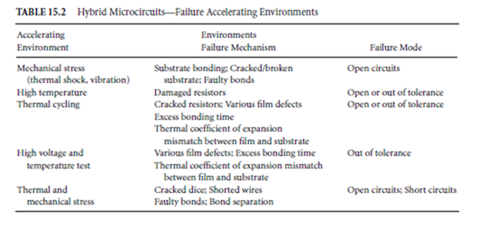
Hybrid devices are a combination of active components (microcircuits or ICs) and various passive discrete parts mounted on a substrate and interconnected by conductive film traces. Hybrid failure mechanisms, like those of discrete and integrated circuits, are primarily due to manufacturing defects. Failures will occur whether the device is operating or dormant. Various accelerating environments, such as temperature or vibration can reveal the failure mechanisms before parts are shipped (or used in circuits). Table 15.2 lists the accelerating environments and the problems they reveal.
Memory IC Failure Modes
Memory ICs failures result in the inability to read or write data, erroneous data storage, unacceptable output levels, and slow access time. The specific failures that cause these problems are as follows:
-
Open and short circuits: can cause various problems from a single bit error to a catastrophic failure of the whole device.
-
LOpen decoder circuits: cause addressing problems to the memory.
-
Multiple writes: writing one cell actually writes to that cell and other cells (multiple write and address uniqueness problems).
-
Pattern sensitivity: the contents of a cell become complemented due to read and write operations in electrically adjacent cells (cell disturbances, adjacent cell disturbances, column disturbances, adjacent column disturbances, row disturbance, adjacent row disturbance).
-
Write recovery: the access time of the device may be slower than specified when each read cycle is preceded by a write cycle, or a number of write cycles.
-
Address decoder switching time: this time can vary depending on the state of the address decoder prior to switching and on the state to which the decoder is switching.
-
Sense amplifier sensitivity: memory information may be incorrect after reading a long series of similar data bits followed by a single transition of the opposite data value.
-
Sleeping sickness: the memory loses information in less than the specified hold time (for DRAMs).
-
Refresh problems (may be static or dynamic): the static refresh test checks the data contents after the device has been inactive during a refresh. In dynamic refresh, the device remains active and some cells are refreshed. All cells are then tested to check whether the data in the nonrefreshed cells is still correct.
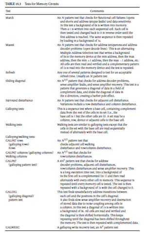
Special tests are needed for memory devices to insure the integrity of every memory bit location. These functional tests are composed of four basic tests, pattern tests, background tests, timing test, and voltage level tests. A summary of these tests is contained in Table 15.3.
Memory tests cannot be specified to test each part 100% as a RAM can contain any one of 2N different data patterns and can be addressed in N factorial (N!) address sequences without using the same address twice. Test times shown may be extremely long for some high-density memory devices; a GALPAT test for a 4 M DRAM would take 106 days to execute. It is easy to see how impractical it is to overspecify device testing. Any test plan should be developed along with the supplier of the memory devices you are to purchase.
System level tests may use bit-map graphics where the status of the memory cells is displayed on the cathode ray tube (CRT) display of the system (i.e., failing bits show up as a wrong color). Various patterns are read into the memory and the CRT may be configured to show 1 cell equivalent to one pixel (a picture element) or compressed to show 4, 16, or 64 cells per pixel depending on the number of pixels available and the memory size. Zoom features can be used to scale the display for close examination of failing areas of the memory.
Note, in large memory intensive systems, consider using error correction codes to correct hard (per- manent failure) and soft errors (i.e., alpha particle upsets, a single upset that does not occur again). One vendor of video RAMs estimates a soft error rate of a 1 Meg part of 3.9 FITs (at a 500-ns cycle time with Vcc at 4.5 V, and a 4 Meg DRAM error rate of 41 FITs (at a 90% confidence level, 5 Vcc operation with 15.625-µs cycle (refresh) rate). Soft error rates are dependent on cycle time and operating voltage; the lower the voltage and faster the cycle time, the higher the failure in time rate. One thousand FITs equals 1 PPM (1 failure in 106 h), which equals 0.1%/1000 (0.1% failures every 1000 h). When calculating soft error rates, add the refresh mode rate and the active mode rate, which can be determined from acceleration curves provided by the manufacturer.
IC Packages and Failures
Devices can be classified by package style, which can either be hermetically sealed (ceramic or metal cans) or nonhermetic (epoxy, silicones, phenolics or plastic encapsulated). Materials employed in most microcircuits will change very slowly if stored in a dry environment at a constant low temperature.
Hermetic packages, glass, ceramic, or metal, protect the device from environmental atmospheric effects. Depending on the metal package it can take anywhere from 50 to well over 100 years for the inside of the IC package to reach 50% of the humidity of the outside air. An epoxy package can take anywhere from minutes to a few days. Therefore, equipment designed for harsh environments, such as might be encountered in military applications, use hermetically sealed devices. Plastic packaged devices are low cost, offer mechanical shock and vibration resistance, are free from loose particles inside the device as they do not have a cavity, and are available in smaller package sizes. All plastics, however, contain some moisture and are permeable to moisture to some degree. (Salt environments have also been shown to effect silicone encapsulated devices but leave epoxy novalac parts relatively unaffected). The mismatch in thermal coefficients of the plastic vs. the die also reduces the operating temperature of the device from 0 to 70◦C vs. hermetic packages, which can operate from −55 to +125◦C.
Studies have been done by the Microelectronics and Computer Technology Corporation (Austin, Texas) and Lehigh University on replacing heremetic packages with more effective lightweight protective coatings. Their program, reliability without hermeticity (RwoH), was initiated by a research contract awarded to them by the U.S. Air Force Wright Laboratory. The RwoH is an industry working group, initiated in
1988, to address nonhermetic electronic packaging issues, specifically, coating to provide environmental protection for semiconductor devices and multichip modules.
The Joint Electron Device Engineering Council (JEDEC) specification A112 defines six levels of mois- ture sensitivity with level 1 being the highest rating, or not moisture sensitive. The other levels are reduced levels, such as level 3, which ensures product integrity (i.e., from popcorning from entraped moisture during soldering) when stored at 30◦C, 85% Rh for 168 h. Level 4 indicates package integrity is ensured for 84 h, and level 6 only permits 6 h of exposure. Plastic parts shipped in sealed bags with desiccant usually are designed for a 12-mo storage and should only be opened when the parts are to be used. Parts stored for longer than this time, especially plastic quad flatpack (PQFP) packaged devices, should be baked to remove the moisture that has entered the package. Entrapped moisture can vaporize during rapid heating, such as in a solder reflow process, and these stresses can cause package cracking. Subsequent high-temperature and moisture exposures can allow contaminants to enter the IC and cause failure at a later time due to corrosion.
Note Hughes Missile Systems reported in 1995 of conditions where organic-based (such as organic acid (OA)) water-soluble fluxes lead to dendrite growth and short circuits. It was found that component seals of high lead glass frit (glass frit is used in cerdip and ceramic flat pack components) and tin and lead on the device leads results in the growth of lead dendrites on the surface of the glass seals. The lead comes from the high lead oxide content of the soft glass itself. High temperatures accelerate the dendrite growth, with shorts occurring in as little as 5 min with 140◦F warm flux. Prevention of this problem includes using different fluxes and minimizing the application of fluxes to the component side of the PC board. Dendrite growth has also been reported for kovar flatpacks stored in foil-lined cardboard packaging. The chlorine dendrite growth, resulting in a high electrical leakage from pins to case, resulted from the chemical impurities in the cardboard and the device. Fiberboard and paperboard packaging is no longer used for device unit packaging. Tin whisker growth also occurs with parts having pure tin plating on the leads.
Specific IC packages have definite failures associated with their use. These include
-
Ball grid array (BGA) or Overmolded pad-array carrier (OMPAC): In manufacture, the primary failure mode for this package is short circuits (98% vs. 2% open circuits).
-
Flip chip: In manufacture, the primary failure mode for a flip chip on an MCM module is a short circuit.
-
PQFP: Packages are susceptible to moisture-induced cracking in applications requiring reflow soldering.
-
Quad flatpack (QFP): The most common quad flatpack manufacturing failure mode is a short circuit (82% short circuits, 2% open circuits, and 16% misalignment problems).
-
Tape carrier package (TCP): Tape automated bonding (TAB) package has an open circuit (98% vs. 2% misalignment problems) failure mode.
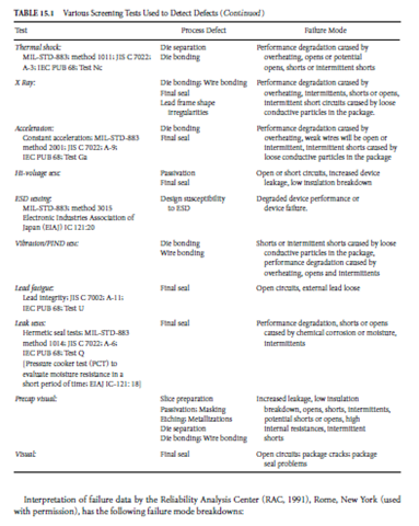
Table 15.1 uses the environmental conditions as screening tests to detect parts that may prematurely fail because of a problem or manufacturing defect. The table shows the various screening tests that can be used to detect the various defects that effect microcircuit reliability. The screens that are rated as good to excellent in identifying component defects, and that are low in cost, are high-temperature storage, temperature cycling, thermal shock, nitrogen bomb test (this tests hermetic package seals), and gross leak test (which also tests hermetic package seals). Screening tests are done prior to putting devices in stock for future use. Proper ESD procedures and controls should be followed, and because of ESD degradation effects the parts should not be periodically handled or tested; only electrically test devices prior to use.
Component failures, such as pin to pin leakage, can also be caused by contaminating films that are on the seal and embedment glass of the package. One such failure mode reported for SRAMs was caused by lead sulfide from antistatic ABS/PVC (acrylonitrile-butadiene-styrene/polyvinyl chloride) plastic trays used to store parts during assembly and postseal operations. The lead sulfide exhibited itself as a shiny film over the seal and embedment glass and resulted in more than 20 µA (at 5 V) leakage. PVC plastic that uses
Thioglycolate (or Dibutyltin bis or Iso Octylthioglicolate, heat stabilizers), a common additive, can cause sulfur-based contamination (and corrosion) on parts with lead-based embedment glass. Because of this, PVC manufacturers are pursuing alternate stabilizer materials, and products that can have performance degradations are often stored and processed using metal trays.
Lead Finish
Reducing lead in the environment is an environmental health and safety issue that is of prime importance today. While a typical microprocessor has approximately 0.2 g of lead and a computer motherboard has 2 to 3 g of lead, and the whole USA electronic interconnection market uses less than 2% of the world’s lead production, to address environmental concerns, there are various environmental directives limiting the use of lead and other hazardous substances. These directives, formulated by the European Union in a Directive of the European parliament and of the Council of the European Union are:
-
End of Life Vehicles (ELV) Directive 2000/53/EC in force since October 21, 2000, requires that products be free of heavy metals such as mercury, cadmium, hexavalent chromium and lead. It requires a recycling system be established by vehicle manufacturers for vehicles made after July 1, 2002 and for all vehicles regardless of date of manufacture by July 1, 2007. Lead can still be used as an alloying additive in copper and in solderable applications.
-
The WEEE Directive, Waste Electrical and Electronic Equipment (WEEE) Directive 2002/96/EC, expands the recycling requirements of the ELV Directive to include a broad range of electronic and electrical appliances and equipment. WEEE went into effect on February 13, 2003. It is to be scheduled to become European national law by August 13, 2004, and be applicable to consumer use products by August 13, 2005. Article 2(3) however states “Equipment which is connected with the protection of the essential interests of the security of Member States, arms, munitions and war material shall be excluded from this Directive. This does not, however, apply to products which are not intended for specifically military purposes.”
-
RoHS Directive, The Restriction of Hazardous Substances in Electrical and Electronic Equipment, this Directive 2002/95/EC establishes standards and limits for the hazardous material content in electronic and electrical equipment. The Directive went into effect on February 13, 2003. It is scheduled to become European national law by August 13, 2004 for be in force for products by July 1, 2006. Banned or restricted substances include lead, mercury, cadmium, hexavalent chromium, certain brominated flame retardants (PBBs), and polybrominated diphenyl ethers (PBDEs).
The recommended lead-free solder formulation is Sn-Ag-Cu for board assembly but there are other formulations such as Nickel-Palladium (NiPd), or Nickel-Palladium with Gold flash (NiPdAu). Passive components, to be compatible with a lower temperature Lead process (which is 215◦C for 50/50 Tin/Lead formulations and 230◦C for 40/60 formulations) and the higher lead-free process of up to 260◦C, use pure matte Tin for their contacts. The use of lead in solder is partially based on several potential reliability issues. Pure Tin component leads have been shown to result in inter-metallic migration in the termination of the electronic component and the growth of tin whiskers which could cause short circuits (which is why there is a exemption for military use (only) components).
The National Electronics Manufacturing Initiative (NEMI) has addressed the problem of “tin whiskers” in lead-free assemblies. A tin whisker is defined by them as A spontaneous columnar or cylindrical filament, which rarely branches, of monocrystalline tin emanating from the surface of a plating finish. Furthermore, tin whiskers may have the following characteristics:
-
an aspect ratio (length/width) greater than 2
-
can be kinked, bent, twisted
-
generally have consistent cross-sectional shape
-
may have striations or rings around it Their recommended test method is
-
temperature cycling (−55◦C to + 85◦C, approximately 3 cycles/hour)
-
temperature humidity tests at 60◦C/93% RH
-
ambient storage (air-conditioned facility)
(Note: Tin will undergo a phase transformation, becoming a powdery form (called Tin Pest) if Tin plated parts are stored for more than 1 week at temperatures below 13◦C).
Screening and Rescreening Tests
In the 1970s, the Navy instituted a policy requiring devices be rescreened on receipt (by the contractor or an independent test laboratory) because there was evidence that Joint Army Navy (JAN) qualified devices (including JANTX, JANTXV discrete component) were not of a quality level to be used in military hardware (DoD directive 4245.7-M Transition from Development to Production, which was signed in 1984 and saw wide implementation by the end of 1986).
Rescreening tests often imposed included the following:
Destructive physical analysis (DPA) examination tests, where two pieces of each lot of parts (as a
minimum) were cut open and examined to determine the workmanship of the parts. If the workmanship
was judged to be poor, the whole lot of parts were rejected (a lot of parts is defined as parts from one
manufacturer from one assembly line and one date code).
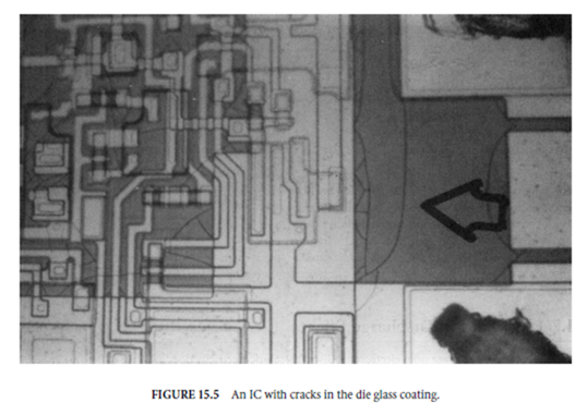
Particle impact noise detection (PIND) tests, where each hybrid part or IC with a cavity where the die was unglassivated (insulated with a glass coating, Fig. 15.5 shows an IC with cracks in this coating), was vibrated and transducers, mounted on the part would detect if there were any particles rattling around.
Parts with loose pieces in them were rejected from the shipment.
Go-no go electrical tests, and static and dynamic tests were required to be performed at low, ambient (25◦C) and high temperatures.
Hermeticity testing was required to test the integrity of the package seal.
 To review the reasons for component rescreening we need to examine test data for the time period involved. In 1981 it was reported that the Naval Weapons Support Center (NWSC) in Crane, Indiana, found part defect rates of 15% for ICs and 17% for discrete semiconductors. In a January 1983 report, one independent test laboratory found reject rates of 16.7% for linear ICs, 8.4% for digital ICs, and 9.2% for CMOS ICs. By October 1984, this same laboratory found defect rates of 5.5% for linear ICs, 3.7% for digital ICs, 8.2% for transistors, and 3.8% for optoelectronics. In 1983, the Defense Electronic Center found semiconductor defect rates of 8% for nonmilitary specification parts, with a less than 1% defect rate for military specification devices. In 1986, a military contractor estimated rescreening failures of 0.9% for ICs and 1.5% for transistors. In 1989, a manufacturer of a special purpose computer workstation for the .S. Navy reported the following rescreening results: IC/semiconductors tested: 8312 (127 types of parts); total rejects PIND/DPA: 25 (16 PIND failures on hybrid components, 6 electrical failures, 3 mechanical failures—broken leads); reject rate: 0.30%.
Breaking down the hybrid failures, of 99 military qualified oscillators tested, 6 were rejected for a rejec- tion rate of 6.1%; 53 nonmilitary qualified oscillators were tested of which 10 were rejected, for a rejection rate of 18.8%.
The Semiconductor Industry of America conducted a quality statistics program to monitor and report on industry data on various quality control indices and parameters of microcircuits from 1985 to the early 1990s. In 1991, the analysis of the data showed that for every 10,000 parts shipped, there is on average only one part with electrical defects, or a 100 parts per million (PPM) defect rate. The data were reported using JEDEC standard 16, Assessment of Microcircuit Outgoing Quality Levels in Parts Per Million and represents data on JAN qualified parts, DESC drawing parts, MIL-STD-883C screened devices, and devices procured to source control drawings (SCDs). Over 150 million devices were sampled with the reporting companies supplying about 80% of all military microcircuits.
The breakdown of defects based upon part type are linear parts: 100 PPM, bipolar digital 50 PPM (10 PPM in the first quarter of 1991), MOS digital: <100 PPM, and MOS memory: 160 PPM (with defects falling an average 30 PPM/quarter). If all the data are combined, the data indicate that for every 25,000 parts shipped, there averages only 1 part with electrical defects. The study also shows that there is a steady and continual decline in the level of electrically defective parts. This analysis shows a significant improvement in part quality since the 1970s, when component rescreening was instituted, and rescreening is probably not necessary except for very high-reliability applications (such as space applications).
Semiconductor, Integrated Circuit, and Hybrid Device Screening Tests
Table 15.1 is a summary of the various screening tests that can be used to detect semiconductor failure mechanisms. Failure mechanisms independent of application environment (oxide or diffusion defects) can be accelerated by operating the device, i.e., performance of a burn-in test.
Failure mechanisms dependent on the application environment (bond or metallization defects) can be accelerated by temperature or mechanical stresses (vibration).
Time and environment dependent failure mechanisms (metal migration, corrosion, intermetallic com- pound formulations caused by dissimilar use) can be accelerated by device operation (i.e., elevated tem- perature burn-in testing).
Electrostatic Discharge Effects
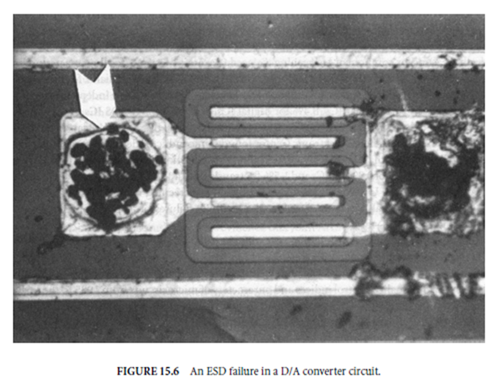
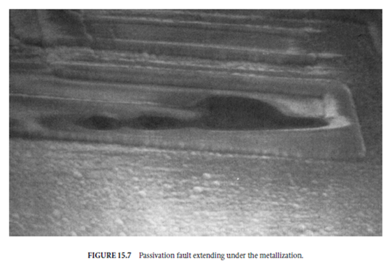
ICs are susceptible to damage from electrostatic discharge. Static electricity does not have to be large enough to cause a visible spark for an IC to be damaged. Figure 15.6 is an ESD failure in a D/A converter circuit. Figure 15.7 shows a passivation fault extending under the metallization.
To prevent ESD damage, various materials are used. Topical antistats, such as those that may be used to coat some plastic IC dip shipping tubes, include detergent substances, which wet the surface being treated. These coatings depend on their moisture content and work most effectively at high humidities. However, these coatings do wear out and treated surfaces must be checked periodically with a static detector.
Treated IC dip tubes should be retreated after use as the IC leads can scrape away the coating as they slide out of the tube.
Pink poly bags are also used to contain components or assemblies. These bags also lose their effectiveness, because they rely on absorbed moisture within the material, and must be checked periodically.
Nickel coated bags may have conductivity discontinuities due to the thin coating cracking after repeated bag handling. These bags should be periodically tested and examined for physical damage.
Defining Terms
Alpha particle: A product given off by the decay of radioactive material (usually emitted by traces of radioactivity in IC ceramic packaging materials). This particle has a positive charge equal to twice that of an electron and is emitted at a very high velocity. Alpha particles can cause temporary memory upsets in DRAMs, which is known as soft error rate.
Bond pad: Areas of metallization on the IC die that permit the connection of fine wires or circuit elements to the die. (See also wire bond.)
Burn-in: Component testing where infant mortality failures (defective or weak parts) are screened out by testing at elevated voltages and temperatures for a specified length of time.
Ceramic: An inorganic, nonmetallic clay or glasslike material whose final characteristics are produced by subjection to high temperatures.
DC test: Tests that measure a static parameter, for example, leakage current.
Defense Electric Supply Center (DESC) part: Used to denote a Standard Military drawing part that has been approved by the DESC, in Columbus (formerly in Dayton), Ohio.
Die: A single IC, also known as a chip.
Die information exchange (DIE): A specification created by chip makers and software vendors to provide basic die information in a standard format.
DIE bonding: The attachment of an IC chip (or DIE) to a substrate or a header.
DIE separation: Refers to the separation of the actual microcircuit chip from the inside of the package.
Destructive physical analysis (DPA): Devices are opened and analyzed for process integrity and workmanship.
Electrostatic discharge (ESD): The instantaneous transfer of charges accumulated on a nonconductor to a conductor, into ground.
Failure in time (FIT): A rating equal to the number of failures in one billion (109) h.
Frit: A relatively low softening point material of glass composition.
Function test: A check for correct device operation generally by truth table verification.
Hermetic: Sealed so that the object is gas tight (usually to a rate of less than 1 × 10⁻⁶ cc/s of helium.)
Joint Army Navy (JAN): When used when referring to microcircuits indicated a part fully qualified to the requirements of MIL-M-38510 for ICs (now replaced by MIL-M-38535) and MIL-S-19500 for semiconductors. JAN class B microcircuit level of the standard military drawing (SMD) program is the preferred level for design in new weapons systems.
JANTX: A prefix denoting that the military specification device has received extra screening and testing, such as an 100% 168-h burn-in.
JANTXV: A JANTX part with an added precapsulation visual requirement.
Joint Electron Device Engineering Council (JEDEC): A part of the EIA.
Lead: A conductive path, usually self-supporting, the portion of an electrical component that connects it to outside circuitry.
Lead frame: The metallic portion of the device package that makes electrical connections from the die to other circuitry.
Mask: The stencil of circuit elements through which light is shown to expose that circuit pattern onto a photoresist coating on the chip (die). The exposed areas are stripped away leaving a pattern.
Metallization: The deposited thin metallic coating layer on a microcircuit or semiconductor.
Passivation: The process in which an insulating dielectric layer is formed over the surface of the die.
Passivation is normally achieved by thermal oxidation of the silicon and a thin layer of silicon dioxide is obtained in this manner (a combination of PECVD oxide and PECVD nitride deposited at lower temperature (below 450◦C)). Other passivation dielectric coatings may also be applied (used), such as silicon glass (silicon oxynitride).
Particle impact noise detection testing (PIND): A test where cavity devices are vibrated and monitored for the presence of loose particles inside the device package via the noise the material makes. These loose particles may be conductive (such as gold flake particles from gold eutectic die attachment operations) and could result in short circuits. This is not required on a 100% basis for military class B devices. It is required for all class S, or devices generally required for spacecraft application use.
Popcorning: A plastic package crack or delamination that is caused by the phase change and expansion of internally condensed moisture in the package during reflow soldering, which results in stress the plastic package can not withstand.
Parts per million (PPM): The number of failures in one million parts. A statistical estimation of the number of defective devices, usually calculated at a 90% confidence level.
Schmoo plot: An X–Y plot giving the pass/fail region for a specific test while varying the parameters in the X and Y coordinates.
Soft error: An error, or upset in the output of a part (usually applies to memory devices for a single bit output error), which does not reoccur (i.e., the device performs to specifications when tested after the failure occurred).
Substrate: The supporting material upon which the microcircuit (IC) is fabricated, or in hybrids the part to which the IC (and other components, etc.) is attached.
Tin whisker: A hairlike single crystal growth formed on the metallization surface.
Wire bond: A wire connection between the semiconductor die bond pad and the leadframe or terminal.
Acknowledgement
I would like to thank Ron Kalakuntla of ISSI (Integrated Silicon Solution Inc.) and Mr. Lawrence Taccour, of Technical Marketing Group, for their assistance in reviewing this chapter.
References
Arnold, H.D. 1981. Institute of Environmental Sciences Proceedings. ESSEH (Environmental Stress Screen- ing of Electronic Hardware), Institute of Environmental Sciences (Mt. Prospect, IL) Conf., Sept. 21.
Bley, W. 1981. Testing high-speed bipolar memories. Fairchild Camera and Instrument Corp., Mountain View, CA, Nov.
CALCE (Computer Aided Life Cycle Engineering) News, Jan. 1993. Workshop On Temperature Effects, University of Maryland, College Park, MD.
Chester, M. 1986. DOD’s rescreening of chips stirs controversy. Electronic Products, Oct. 15, pp. 83–84. Costlow, T. 1995. MCM substrates mixed. Electronic Engineering Times, Jan. 16.
Ellis, M. 1984. Non-Mil Defects Surpass Mil. Electronic Buyers’ News, Nov. 26, p. 6.
Frye, M.A. 1994. Extension of the implementation date of MIL-I-38535 and MIL-S-19500 regarding the prohibition of pure tin as a plating material. Defense Logistics Agency, Defense Electronics Supply Center, Dayton, OH (Letter dated Jan. 21).
GIDEP. Government and Industry Data Exchange Program (Corona, CA), Problem Advisory, 7G-P-95- 01 (Jan. 1995), Microcircuits, Flux, Soldering, Liquid; Problem Advisory,G4-P-93-01, Packaging, Cardboard, Flatpack, Microcircuit; Problem Advisory, ZW-P- 9301A (Jan. 1993), Storage Container, Material, Contamination; Problem Advisory, S4-P-93-01 (Jan. 1993), Transistor, Tin Plating, Whisker Growth.
Gulley, D.W. 1992. Texas Instruments, mean time between events, a discussion of device failures in DRAMs. 9(5), Sept.
Hamilton, H.E. 1984. Electronics test. Micro Control Co. Minneapolis, MN, April.
Hitachi. 1991. Reliability report, Multiport Video RAM. HM534251, MC-883, Hitachi, Ltd., Tokyo, Japan, Oct. 14.
Hnatek, E.R. 1983. The case for component rescreening. Test & Measurement World, Jan., pp. 18–24.
Hnatek, E.R. 1984. ICs for military and aerospace show dramatic jump in quality, reliability, military/space electronics design. Viking Labs., Inc. Military/Space Electronics Design (McGraw-Hill), Oct., pp. 27– 30.
Hu, J.M., Barker, D., Dasgupta, A., and Arora, A. 1993. Role of failure-mechanism identification in accelerated testing. Journal of the IES (July/Aug.), Institute of Environmental Sciences (Mt. Prospect, IL).
ESSEH (Environmental Stress Screening of Electronic Hardware) 1985. Environmental stress screening for parts. Institute of Environmental Sciences Proceedings, ESSEH, Sept.
Klinger, D.J., Nakada, Y., and Memendez, M.A. AT&T Reliability Manual, Van Nostrand Reinhold,1990.
Lawrence, J.D. Jr. 1983. Parallel testing of memory devices. Reliability Inc., Houston, TX, Oct.
RADC. 1988. Reliability/maintainability/testability design for dormancy. Lockheed Electronics Co., Rome Air Development Center, Rept. RADC-TR-88-110, May. (Available from the Defense Technical Information Center (document #AD-A202-704)), Defense Logistics Agency, Department of Defense.
Meeldijk, V. 1995. Electronic Components: Selection and Application Guidelines. Wiley Interscience, New York, Chap. 10 and 11.
Meeldijk, V. 1990. Effects of storage and dormancy on components. Electronic Servicing and Technology Magazine, Dec., pp. 6–11.
Micron Technology, Inc., Boise, ID. 1991. Quality/Reliability Handbook, 4/91, Reliability Monitor, 4 M DRAM, rev. 10/91 and 1 MEG DRAM book.
MIL-HDBK. 1988. Electronic Reliability Design Handbook. MIL-HDBK-338 Military Handbook, Oct. 12.
MIL-STD. 1995. NASA standard electrical, electronic, and electromechanical (EEE) parts list. MIL-STD- 975, March 17.
MIL-STD. 1992. Electronic parts, materials, and processes for space and launch vehicles. MIL-STD-1547, Dec. 1.
MIL-STD-19500. 1994. General specification for semiconductor devices, April 15.
Motorola, Phoenix, AZ. 1982. Dynamic RAM quality and reliability report. MCM6664A/6665A 64K.
Murray, J. 1994. MCMs pose many production problems. Electronic Engineering Times, June 11.
Navsea Systems Command. 1991. Washington, D.C. Parts application and reliability information manual for Navy electronic equipment. TE000-AB-GTP-010, Navsea Systems Command (stock number 0910- LP-494-5300), March.
O’Connor, P.T.D. 1985. Practical Reliability Engineering, 2nd ed. Wiley, New York.
RAC. 1991. Failure mode/mechanism distributions. FMD-91, Reliability Analysis Center, Rome, NY.
School, R. 1985. Effective screening techniques for dynamic RAMs. Pacific Reliability Corp. presented at Electro., Institute of Electrical and Electronic Engineers.
Schaefer, S. 1994. DRAM soft error rate calculations. Design Line, 3(1).
Semiconductor Industry Association (San Jose, CA). 1991. Quality statistics report on military integrated circuits. Government Procurement Committee.
Smith, D.J. 1985. Reliability and Maintainability in Perspective, 2nd ed. Halsted Press, Wiley, New York.
Somos, I.L., Eriksson, L.O., and Tobin, W.H. 1986. Understanding di/dt ratings and life expectancy for thyristors. PCIM Magazine, Feb.
U.S. Army Material Command AMCP-706-196.
Willoughby, W.J. Jr. 1980. Military electronics/countermeasures: View from the top (interview), Aug., pp. 14–20, 60–61.
Yalamanchili, P., Gannamani,R., Munamarty, R., McClusky, P., and Christou, A. 1995. Optimum processing prevents PQFP popcorning. CALCE Electronic Packaging Research Center, MD, SMT, May.
Semiconductor Failure Modes 15-19
Further Information
The following sources can be referenced for additional data on failure modes:
The Reliability Analysis Center (RAC), Rome, NY, Failure Mode/Mechanism Distributions, 1991, FMD-91.
AT&T Reliability Manual, by David J. Klinger, Yoshinao Nakada, and Maria A. Memendez, published by Van Nostrand Reinhold, 1990.

