Transmission Lines

Introduction

A transmission line is a system of conductors connecting one point to another and along which electromagnetic energy can be sent. Thus telephone lines and power distribution lines are typical examples of transmission lines; in electronics, however, the term usually implies a line used for the transmission of radio-frequency (r.f.) energy such as that from a radio transmitter to the antenna.

An important feature of a transmission line is that it should guide energy from a source at the sending end to a load at the receiving end without loss by radiation. One form of construction often used consists of two similar conductors mounted close together at a constant separation. The two conductors form the two sides of a balanced circuit and any radiation from one of them is neutralised by that from the other. Such twin-wire lines are used for carrying high r.f. power, for example, at transmitters. The coaxial form of construction is commonly employed for low power use, one conductor being in the form of a cylinder that surrounds the other at its centre, and thus acts as a screen. Such cables are often used to couple f.m. and television receivers to their antennas.

At frequencies greater than 1000 MHz, transmission lines are usually in the form of a waveguide, which may be regarded as coaxial lines without the centre conductor, the energy being launched into the guide or abstracted from it by probes or loops projecting into the guide.

Transmission Line Primary Constants

Let an a.c. generator be connected to the input terminals of a pair of parallel conductors of infinite length. A sinusoidal wave will move along the line and a finite current will flow into the line. The variation of voltage with distance along the line will resemble the variation of applied voltage with time. The moving wave, sinusoidal in this case, is called a voltage travelling wave. As the wave moves along the line the capacitance of the line is charged up and the moving charges cause magnetic energy to be stored. Thus the propagation of such an electromagnetic wave constitutes a flow of energy.

After sufficient time the magnitude of the wave may be measured at any point along the line. The line does not therefore appear to the generator as an open circuit but presents a definite load Z0. If the sending-end voltage is VS and the sending end current is image. Thus, the line absorbs all of the energy and the line behaves in a similar manner to the generator, as would a single ‘lumped’ impedance of value Z0 connected directly across the generator terminals.

There are four parameters associated with transmission lines, these being resistance, inductance, capacitance and conductance.

(i) Resistance R is given by R + pl/A, where p is the resistivity of the conductor material, A is the cross-sectional area of each conductor and l is the length of the conductor (for a two-wire system, l represents twice the length of the line). Resistance is stated in ohms per metre length of a line and represents the imperfection of the conductor. A resistance stated in ohms per loop metre is a little more specific since it takes into consideration the fact that there are two conductors in a particular length of line.

(ii) Inductance L is due to the magnetic field surrounding the conductors of a transmission line when a current flows through them. The inductance

of an isolated twin line is considered in chapter 79. From equation (11), image henry/ metre, where D is the distance between centres of the conductor and a is the radius of each conductor. In most practical lines µr D 1. An inductance stated in henrys per loop metre takes into consideration the fact that there are two conductors in a particular length of line.

(iii) Capacitance C exists as a result of the electric field between conductors of a transmission line. The capacitance of an isolated twin line is considered in chapter 79. From equation (7), page 594, the capacitance between the two conductors is given by: image farads/metre. In most practical lines εr D 1.

(iv) Conductance G is due to the insulation of the line allowing some current to leak from one conductor to the other. Conductance is measured in siemens per metre length of line and represents the imperfection of the insulation. Another name for conductance is leakance.

Each of the four transmission line constants, R, L, C and G, known as the primary constants, are uniformly distributed along the line.

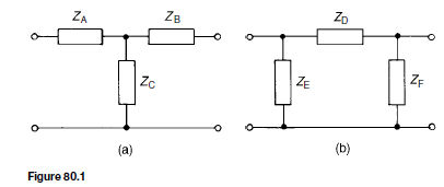
From chapter 80, when a symmetrical T-network is terminated in its characteristic impedance Z0, the input impedance of the network is also equal to Z0. Similarly, if a number of identical T-sections are connected in cascade, the input impedance of the network will also be equal to Z0.

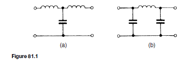
A transmission line can be considered to consist of a network of a very large number of cascaded T-sections each a very short length (υl) of transmission line, as shown in Figure 83.1. This is an approximation of the uniformly distributed line; the larger the number of lumped parameter sections, the nearer

image

it approaches the true distributed nature of the line. When the generator VS is connected, a current IS flows which divides between that flowing through the leakage conductance G, which is lost, and that which progressively charges each capacitor C and which sets up the voltage travelling wave moving along the transmission line. The loss or attenuation in the line is caused by both the conductance G and the series resistance R.

Phase Delay, Wavelength and Velocity of Propagation

Each section of that shown in Figure 83.1 is simply a low-pass filter possessing losses R and G. If losses are neglected, and R and G are removed, the circuit simplifies and the infinite line reduces to a repetitive T-section low-pass filter network as shown in Figure 83.2. Let a generator be connected to the line as shown and let the voltage be rising to a maximum positive value just at the instant when the line is connected to it. A current IS flows through inductance L1 into capacitor C1. The capacitor charges and a voltage develops across it. The voltage sends a current through inductance L0 and L2 into capacitor

C2. The capacitor charges and the voltage developed across it sends a current through L0 and L3 into C3, and so on. Thus all capacitors will in turn charge up to the maximum input voltage. When the generator voltage falls, each capacitor is charged in turn in opposite polarity, and as before the input charge is progressively passed along to the next capacitor. In this manner voltage and current waves travel along the line together and depend on each other.

The process outlined above takes time; for example, by the time capacitor C3 has reached its maximum voltage, the generator input may be at zero or moving towards its minimum value. There will therefore be a time, and thus a phase difference between the generator input voltage and the voltage at any point on the line.

Phase delay

Since the line shown in Figure 83.2 is a ladder network of low-pass T-section filters, it may be shown that the phase delay, ˇ, is given by:

image

Wavelength

The wavelength A on a line is the distance between a given point and the next point along the line at which the voltage is the same phase, the initial point leading the latter point by 2ˇ radian. Since in one wavelength a phase change of 2ˇ radians occurs, the phase change per metre is image Hence, phase change per metre,

image

Velocity of propagation

The velocity of propagation, u, is given by u D fA, where f is the frequency and A the wavelength. Hence

image

The velocity of propagation of free space is the same as that of light, i.e. approximately 300 x 106 m/s. The velocity of electrical energy along a line is always less than the velocity in free space. The wavelength A of radiation in free space is given by A + f where c is the velocity of light. Since the velocity along a line is always less than c, the wavelength corresponding to any particular frequency is always shorter on the line than it would be in free space.

For example, a transmission line has an inductance of 4 mH/loop km and a capacitance of 0.004 µF/km. For a frequency of operation of 1 kHz, from

image

Current and Voltage Relationships

Figure 83.3 shows a voltage source VS applied to the input terminals of an infinite line, or a line terminated in its characteristic impedance, such that a current IS flows into the line. At a point, say, 1 km down the line let the current be I1 . The current I1 will not have the same magnitude as IS because of line attenuation; also I1 will lag IS by some angle ˇ. The ratio image is therefore a phasor quantity. Let the current a further 1km down the line be I2 , and so on, as shown in Figure 83.3. Each unit length of line can be treated as a section of a repetitive network, and the attenuation is in the form of a

image

where y is the propagation constant. y has no unit.

The propagation constant is a complex quantity given by y = a+jB where ˛ is the attenuation constant, whose unit is the neper, and ˇ is the phase shift coefficient, whose unit is the radian. For n such 1 km sections,

image

In equation (4), the attenuation on the line is given by n˛ nepers and the phase shift is nˇ radians.

At all points along an infinite line, the ratio of voltage to current is Z0, the characteristic impedance. Thus from equation (4) it follows that: receiving end voltage,

image

Characteristic Impedance and Propagation Coefficient in Terms of the Primary Line Constants

At all points along an infinite line, the ratio of voltage to current is called the characteristic impedance Z0. The value of Z0 is independent of the length of the line; it merely describes a property of a line that is a function of the physical construction of the line. Since a short length of line may be considered as a ladder of identical low-pass filter sections, the characteristic impedance may be determined from chapter 80, i.e.

image

since the open-circuit impedance ZOC and the short-circuit impedance ZSC may be easily measured.

The characteristic impedance of a transmission line may also be expressed in terms of the primary constants, R, L, G and C. Measurements of the primary constants may be obtained for a particular line and manufacturers usually state them for a standard length.

It may be shown that the characteristic impedance Z0 is given by:

image

image

Distortion on Transmission Lines

If the waveform at the receiving end of a transmission line is not the same shape as the waveform at the sending end, distortion is said to have occurred.

In designing a transmission line, if LG = CR no distortion is introduced. This means that the signal at the receiving end is the same as the sending-end signal except that it is reduced in amplitude and delayed by a fixed time. Also, with no distortion, the attenuation on the line is a minimum.

In practice, however, The inductance is usually low and the capacitance is large and not easily reduced. Thus if the condition LG D CR is to be achieved in practice, either L or G must be increased since neither C or R can really be altered. It is undesirable to increase G since the attenuation and power losses increase. Thus the inductance L is the quantity that needs to be increased and such an artificial increase in the line inductance is called loading. This is achieved either by inserting inductance coils at intervals along the transmission line — this being called ‘lumped loading’ — or by wrapping the conductors with a high-permeability metal tape — this being called ‘continuous loading

image

Wave Reflection and Reflection Coefficient

In earlier sections of this chapter it was assumed that the transmission line had been properly terminated in its characteristic impedance or regarded as an infinite line. In practice, of course, all lines have a definite length and often the terminating impedance does not have the same value as the characteristic

impedance of the line. When this is the case, the transmission line is said to have a ‘mismatched load’.

The forward-travelling wave moving from the source to the load is called the incident wave or the sending-end wave. With a mismatched load the termination will absorb only a part of the energy of the incident wave, the remainder being forced to return back along the line toward the source. This latter wave is called the reflected wave.

A transmission line transmits electrical energy; when such energy arrives at a termination that has a value different from the characteristic impedance, it experiences a sudden change in the impedance of the medium. When this occurs, some reflection of incident energy occurs and the reflected energy is lost to the receiving load. Reflections commonly occur in nature when a change of transmission medium occurs; for example, sound waves are reflected at a wall, which can produce echoes (see Chapter 17), and mirrors reflect light rays (see Chapter 19).

If a transmission line is terminated in its characteristic impedance, no reflection occurs; if terminated in an open circuit or a short circuit, total reflection occurs, i.e. the whole of the incident wave reflects along the line. Between these extreme possibilities, all degrees of reflection are possible.

Energy associated with a travelling wave

A travelling wave on a transmission line may be thought of as being made up of electric and magnetic components. Energy is stored in the magnetic field due to the current (energy D 1 LI2 — see page 597) and energy is stored in the electric field due to the voltage (energy D 1 CV2 — see page 594). It is the continual interchange of energy between the magnetic and electric fields, and vice versa, that causes the transmission of the total electromagnetic energy along the transmission line.

When a wave reaches an open-circuited termination the magnetic field collapses since the current I is zero. Energy cannot be lost, but it can change form. In this case it is converted into electrical energy, adding to that already caused by the existing electric field. The voltage at the termination consequently doubles and this increased voltage starts the movement of a reflected wave back along the line. This movement will set up a magnetic field and the total energy of the reflected wave will again be shared between the magnetic and electric field components.

When a wave meets a short-circuited termination, the electric field col- lapses and its energy changes form to the magnetic energy. This results in a doubling of the current.

Reflection coefficient

The ratio of the reflected current to the incident current is called the reflection coefficient and is often given the symbol p, i.e.

image

image

For example, a cable, which has a characteristic impedance of 75 ω, is terminated in a 250 ω resistive load. Assume that the cable has negligible losses and the voltage measured across the terminating load is 10 V.

From equation (11), reflection coefficient,

image

Standing Waves and Standing Wave Ratio

Consider a loss free transmission line open-circuited at its termination. An incident current waveform is completely reflected at the termination, and, as stated in earlier, the reflected current is of the same magnitude as the incident

image

current but is 180° out of phase. Figure 83.5(a) shows the incident and reflected current waveforms drawn separately (shown as Ii moving to the right and Ir moving to the left respectively) at a time t D 0, with Ii D 0 and decreasing at the termination.

The resultant of the two waves is obtained by adding them at intervals. In this case the resultant is seen to be zero. Figures 83.5(b) and (c) show the incident and reflected waves drawn separately as times t D T/8 seconds and t D T/4, where T is the periodic time of the signal. Again, the resul- tant is obtained by adding the incident and reflected waveforms at intervals. Figures 83.5(d) to (h) show the incident and reflected current waveforms plot- ted on the same axis, together with their resultant waveform, at times t D 3T/8 to t D 7T/8 at intervals of T/8.

If the resultant waveforms shown in Figures 83.5(a) to (g) are superimposed one upon the other, Figure 83.6 results. (Note that the scale has been doubled for clarity.) The waveforms show clearly that waveform (a) moves to (b) after T/8, then to (c) after a further period of T/8, then to (d), (e), (f), (g) and (h) at intervals of T/8. It is noted that at any particular point the cur- rent varies sinusoidally with time, but the amplitude of oscillation is different at different points on the line.

Whenever two waves of the same frequency and amplitude travelling in opposite directions are superimposed on each other as above, interference takes place between the two waves and a standing or stationary wave is produced. The points at which the current is always zero are called nodes (labelled N in Figure 83.6). The standing wave does not progress to the left or right and the nodes do not oscillate. Those points on the wave that undergo maximum distur- bance are called antinodes (labelled A in Figure 83.6). The distance between adjacent nodes or adjacent antinodes is A/2, where A is the wavelength. A standing wave is therefore seen to be a periodic variation in the vertical plane taking place on the transmission line without travel in either direction The resultant of the incident and reflected voltage for the open-circuit termination may be deduced in a similar manner to that for current. However, as stated earlier, when the incident voltage wave reaches the termination it is reflected without phase change. Figure 83.7 shows the resultant waveforms of incident and reflected voltages at intervals of t D T/8. Figure 83.8 shows all the resultant waveforms of Figure 83.7(a) to (h) superimposed; again, standing waves are seen to result. Nodes (labelled N) and antinodes (labelled A) are

image

image

image

shown in Figure 83.8 and, in comparison with the current waves, are seen to occur 90° out of phase.

If the transmission line is short-circuited at the termination, it is the incident current that is reflected without phase change and the incident voltage that is reflected with a phase change of 180° . Thus the diagrams shown in Figures 83.5 and 83.6 representing current at an open-circuited termination may be used to represent voltage conditions at a short-circuited termination and the diagrams shown in Figures 83.7 and 83.8 representing voltage at an open-circuited termination may be used to represent current conditions at a short-circuited termination.

Figure 83.9 shows the r.m.s. current and voltage waveforms plotted on the same axis against distance for the case of total reflection, deduced from Figures 83.6 and 83.8. The r.m.s. values are equal to the amplitudes of the waveforms shown in Figures 83.6 and 83.8, except that they are each divided

image

total reflection, the standing-wave patterns of r.m.s. voltage and current consist of a succession of positive sine waves with the voltage node located at the current antinode and the current node located at the voltage antinode. The termination is a current nodal point. The r.m.s. values of current and voltage may be recorded on a suitable r.m.s. instrument moving along the line. Such measurements of the maximum and minimum voltage and current can provide a reasonably accurate indication of the wavelength, and also provide information regarding the amount of reflected energy relative to the incident energy that is absorbed at the termination, as shown below.

image

Standing-wave ratio

Let the incident current flowing from the source of a mismatched low-loss transmission line be Ii and the current reflected at the termination be Ir . If IMAX is the sum of the incident and reflected current, and IMIN is their difference, then the standing-wave ratio (symbol s) on the line is defined as:

image


Attenuators

Introduction

An attenuator is a device for introducing a specified loss between a signal source and a matched load without upsetting the impedance relationship necessary for matching. The loss introduced is constant irrespective of frequency; since reactive elements (L or C) vary with frequency, it follows that ideal attenuators are networks containing pure resistances. A fixed attenuator section is usually known as a ‘pad’.

Attenuation is a reduction in the magnitude of a voltage or current due to its transmission over a line or through an attenuator. Any degree of attenuation may be achieved with an attenuator by suitable choice of resistance values but the input and output impedances of the pad must be such that the impedance conditions existing in the circuit into which it is connected are not disturbed. Thus an attenuator must provide the correct input and output impedances as well as providing the required attenuation.

Two-port Networks

Networks in which electrical energy is fed in at one pair of terminals and taken out at a second pair of terminals are called two-port networks. Thus an attenuator is a two-port network, as are transmission lines, transformers and electronic amplifiers. If a network contains only passive circuit elements, such as in an attenuator, the network is said to be passive; if a network contains a source of e.m.f., such as in an electronic amplifier, the network is said to be active.

Figure 80.1(a) shows a T-network, which is termed symmetrical if ZA D ZB and Figure 80.1(b) shows a .r-network which is symmetrical if ZE= ZF. If ZA 6D ZB in Figure 80.1(a), and ZE 6D ZF in Figure 80.1(b), the sections are termed asymmetrical. Both networks shown have one common terminal, which may be earthed, and are therefore said to be unbalanced. The balanced

image

image

form of the T-network is shown in Figure 80.2(a) and the balanced form of the .r-network is shown in Figure 80.2(b).

Characteristic Impedance

The input impedance of a network is the ratio of voltage to current (in complex form) at the input terminals. With a two-port network the input impedance often varies according to the load impedance across the output terminals. For any passive two-port network it is found that a particular value of load impedance can always be found which will produce an input impedance having the same value as the load impedance. This is called the iterative impedance for an asymmetrical network and its value depends on which pair of terminals is taken to be the input and which the output (there are thus two values of iterative impedance, one for each direction). For a symmetrical network there is only one value for the iterative impedance and this is called the characteristic impedance of the symmetrical two-port network.

Logarithmic Ratios

The ratio of two powers P1 and P2 may be expressed in logarithmic form as shown in chapter 50. Let P1 be the input power to a system and P2 the output power.

If logarithms to base 10 are used then

image

For example, if, say, 5% of the power supplied to a cable appears at the output terminals then the attenuation in decibels is determined as follows:

From equation (1),

image

Hence the attenuation (i.e. power loss) is 13 dB.

In another example, if an amplifier has a gain of 15 dB and the input power is 12 mW, the output power is determined as follows:

From equation (1),

image

The attenuation of filter sections and along a transmission line are of an exponential form and it is in such applications that the unit of the neper is used (see chapters 81 and 83).

Symmetrical T -attenuator

For the symmetrical T-pad attenuator is shown in Figure 80.3, the characteristic impedance R0 is given by:

image

image

For example, a T-section symmetrical attenuator pad to provide a voltage attenuation of 20 dB and having a characteristic impedance of 600 Q is designed as follows:

image

image

Symmetrical p-attenuator

For the symmetrical .r-attenuator shown in Figure 80.4 the characteristic impedance R0 is given by:

image

For example, if a .r-section symmetrical attenuator is required to provide a voltage attenuation of 25 dB and have a characteristic impedance of 600 Q, then:

image

Insertion Loss

Figure 80.5(a) shows a generator E connected directly to a load ZL . Let the current flowing be IL and the p.d. across the load VL . z is the internal impedance of the source.

Figure 80.5(b) shows a two-port network connected between the generator E and load ZL . The current through the load, shown as I2 , and the p.d. across the load, shown as V2 will generally be less than current IL and voltage VL of Figure 80.5(a), as a result of the insertion of the two-port network between generator and load.

image

image

When the two-port network is terminated in its characteristic impedance Z0 the network is said to be matched. In such circumstances the input impedance is also Z0, thus the insertion loss is simply the ratio of input to output voltage

image

For example, a 0– 3 kQ rheostat is connected across the output of a signal generator of internal resistance 500 Q. If a load of 2 kQ is connected across the rheostat, the insertion loss at a tapping of, say, 2 kQ is determined as follows:

The circuit diagram is shown in Figure 80.6. Without the rheostat in the ircuit the voltage across the 2 kQ load, VL (see Figure 80.7), is given by:

image

With the 2 kQ tapping, the network of Figure 80.7 may be redrawn as shown in Figure 80.8, which in turn is simplified as shown in Figure 80.9. From Figure 80.9,

image

image

Asymmetrical T – and p-sections

Figure 80.10(a) shows an asymmetrical T-pad section where resistance R1 6D 3. Figure 80.10(b) shows an asymmetrical .r-section where R2 6D R3.

When viewed from port A, in each of the sections, the output impedance is ROB; when viewed from port B, the input impedance is ROA. Since the sections are asymmetrical ROA does not have the same value as ROB.

Iterative impedance is the term used for the impedance measured at ne port of a two-port network when the other port is terminated with an impedance of the same value. For example, the impedance looking into port 1 of Figure 80.11(a) is, say, 500 Q when port 2 is terminated in 500 Q and the impedance looking into port 2 of Figure 80.11(b) is, say, 600 Q when port 1 is terminated in 600 Q. (In symmetric T- and .r-sections the two iterative impedances are equal, this value being the characteristic impedance of the section).

An image impedance is defined as the impedance which, when connected to the terminals of a network, equals the impedance presented to it at the opposite terminals. For example, the impedance looking into port 1 of Figure 80.12(a) is, say, 400 Q when port 2 is terminated in, say 750 Q, and the impedance seen looking into port 2 (Figure 80.12(b)) is 750 Q when port

image

image

1 is terminated in 400 Q. An asymmetrical network is correctly terminated when it is terminated in its image impedance. (If the image impedances are equal, the value is the characteristic impedance).

For example, an asymmetrical T-section attenuator is shown in Figure 80.13. The image and iterative impedances are determined as follows: The image impedance ROA seen at port 1 in Figure 80.13 is given by equation (4): imagewhere ROC and RSC refer to port 2 being respectively open-circuited and short circuited.

image

image

image

Thus the iterative impedances of the section shown in Figure 80.13 are 285.4  and 385.4

The L-section Attenuator

For the L-section attenuator shown in Figure 80.16,

image

Two-port Networks in Cascade

Often two-port networks are connected in cascade, i.e. the output from the first network becomes the input to the second network, and so on, as shown in Figure 80.17. Thus an attenuator may consist of several cascaded sections so as to achieve a particular desired overall performance.

If the cascade is arranged so that the impedance measured at one port and the impedance with which the other port is terminated have the same

image

value, then each section (assuming they are symmetrical) will have the same characteristic impedance Z0 and the last network will be terminated in Z0. Thus each network will have a matched termination and hence the attenuation

image


Modulation

Introduction to Modulation

The transmission of information such as speech, music and data over long distances requires the use of a carrier channel. It is common practise to ‘carry’ different communications, called signals, at different frequencies to stop one signal from interfering with another. A signal can be shifted bodily from its original band to another, this being achieved by ‘modulating’ one waveform with another.

The mean frequency level to which a signal is moved is called the carrier frequency and the process of superimposing the information signal on the carrier is called modulation. The resultant signal is called the modulated signal. Many signals, such as telephone conversations, can be transmitted simultaneously along a single pair of lines by using modulation techniques. Modulation of a band of low frequencies on to a higher frequency carrier is fundamental to radio communications, and using different carrier frequencies leads to numerous programmes being transmitted simultaneously. The carrier frequency is the frequency to which the receiver has to be tuned, for example, 97.6 to 99.8 MHz for BBC Radio 1, the signal which is heard being obtained from the modulated carrier by a process called demodulation.

Amplitude Modulation

The carrier frequency must have one or more of its characteristics (i.e. amplitude, frequency and/or phase) varied by the information signal. When the amplitude of the carrier is changed by the information signal, the process is called amplitude modulation. To illustrate amplitude modulation, consider the signal to be a sine wave of frequency fm , as shown in Figure 82.1(a), and the carrier to be a sine wave of frequency fc , as shown in Figure 82.1(b). The result of amplitude modulation is shown in Figure 82.1(c), the signal information being duplicated on both sides of the carrier, as shown by the broken lines, which are construction lines outlining the pattern of change of amplitude of the modulated waveform. This results in a band of frequencies over a range (fc – fm ) to (fc + fm ), i.e. the carrier frequency š the signal frequency band. The frequency range between the highest and lowest of these frequencies is called the bandwidth.

Frequency Modulation

Instead of varying the amplitude of the carrier waveform, the modulating signal may be used to vary the frequency of the carrier. An increase in signal

image

amplitude then causes a change in the modulated signal frequency, which is proportional to the amplitude of the modulating signal. This is called frequency modulation and is shown for a cosine wave signal in Figure 82.2.

When the signal amplitude is positive, the frequency of the carrier is modulated to be less than it was originally, shown as (a). The original carrier is shown for reference. The modulated wave is in the same position as the

image

original carrier when the signal amplitude is zero, as shown at (b). When the signal amplitude is negative, the frequency of the carrier is modulated to be greater than that of the original carrier, as shown at (c).

Frequency Deviation, Frequency Swing and Modulating Index

Frequency deviation is a term used in frequency modulation and is defined as the peak difference between the instantaneous frequency of the modulated wave and the carrier frequency during one cycle of modulation.

Frequency swing is the difference between the maximum and minimum values of the instantaneous frequency of a frequency-modulated wave.

The modulating index for a sinusoidal modulating waveform is the ratio of frequency deviation to the frequency of the modulating wave. Thus the modulating index is the ratio of the frequency deviation caused by a particular signal to the frequency of that signal.

Phase Modulation

The modulating signal can be used to advance or retard the phase of the carrier in proportion to the amplitude of the modulating signal. This technique is called phase modulation and this also involves a variation of frequency. In this case it depends on the rate of change of phase and thus on both the

image

amplitude and frequency of the modulating signal. The waveform is similar to that shown in Figure 82.2.

Pulse Modulation

In pulse modulation, the signal is sampled at a frequency that is at least twice that of the highest frequency present in the signal. Thus for speech, which has frequencies ranging from about 300 Hz to 3.4 kHz, a typical sampling frequency is 8 kHz. Various forms of pulse modulation are used and include pulse amplitude modulation, pulse position modulation and pulse duration modulation.

The principle of pulse modulation is shown in Figure 82.3(a), in which the amplitude of the pulse is proportional to the amplitude of the signal. The amplitude of the pulse may change during the ‘on’ period or alternatively it may be kept constant, resulting in the stepped waveform as shown in Figure 82.3(a).

image

Figure 82.3(b) shows the principle of pulse duration modulation, the duration of the pulse being proportional to the amplitude of the signal.

The position of the pulse relative to some datum (such as the sampling time), is made proportional to the amplitude of the signal in pulse position modulation, as shown in Figure 82.3(c).

Pulse Code Modulation

In pulse code modulation, the signal amplitude is divided into a number of equal increments, each increment being designated by a number. For example, an amplitude divided into eight increments can have the instantaneous value of the amplitude transmitted by using the natural binary numbering system with three bits, the level being transmitted as: 000, 001, 011,.. ., 111. This concept is shown in Figure 82.4.

Thus in pulse code modulation, an analogue signal is converted into a digital signal. Since the analogue signal can have any value between certain limits, but the resulting digital signal has only discrete values, some distortion of the signal results. The greater the number of increments, the more closely the digital signal resembles the analogue signal.


Filter Networks

Introduction

A filter is a network designed to pass signals having frequencies within certain bands (called passbands) with little attenuation, but greatly attenuates signals within other bands (called attenuation bands or stopbands).

A filter is frequency sensitive and is thus composed of reactive elements. Since certain frequencies are to be passed with minimal loss, ideally the inductors and capacitors need to be pure components since the presence of resistance results in some attenuation at all frequencies.

Between the pass band of a filter, where ideally the attenuation is zero, and the attenuation band, where ideally the attenuation is infinite, is the cut- off frequency, this being the frequency at which the attenuation changes from zero to some finite value.

A filter network containing no source of power is termed passive, and one containing one or more power sources is known as an active filter network.

Filters are used for a variety of purposes in nearly every type of electronic communications and control equipment. The bandwidths of filters used in communications systems vary from a fraction of a hertz to many megahertz,

depending on the application.

There are four basic types of filter sections:

(a) low-pass

(b) high-pass

(c) band-pass

(d) band-stop

Low-pass Filters

Figure 81.1 shows simple unbalanced T- and n-section filters using series inductors and shunt capacitors. If either section is connected into a net- work and a continuously increasing frequency is applied, each would have a frequency-attenuation characteristic as shown in Figure 81.2. This is an ideal characteristic and assumes pure reactive elements. All frequencies are seen

image

image

to be passed from zero up to a certain value without attenuation, this value being shown as fC, the cut-off frequency; all values of frequency above fC are attenuated. It is for this reason that the networks shown in Figures 81.1(a) and (b) are known as low-pass filters.

The electrical circuit diagram symbol for a low-pass filter is shown in Figure 81.3.

Summarising, a low-pass filter is one designed to pass signals at frequencies below a specified cut-off frequency.

In practise, the characteristic curve of a low-pass prototype filter section looks more like that shown in Figure 81.4. The characteristic may be improved somewhat closer to the ideal by connecting two or more identical sections in cascade. This produces a much sharper cut-off characteristic, although the attenuation in the pass band is increased a little.

When rectifiers are used to produce the d.c. supplies of electronic systems, a large ripple introduces undesirable noise and may even mask the effect of the

image

signal voltage. Low-pass filters are added to smooth the output voltage wave- form, this being one of the most common applications of filters in electrical circuits.

Filters are employed to isolate various sections of a complete system and thus to prevent undesired interactions. For example, the insertion of low- pass decoupling filters between each of several amplifier stages and a common power supply reduces interaction due to the common power supply impedance.

High-pass Filters

Figure 81.5 shows simple unbalanced T- and n-section filters using series capacitors and shunt inductors. If either section is connected into a network and a continuously increasing frequency is applied, each would have a frequency- attenuation characteristic as shown in Figure 81.6.

Once again this is an ideal characteristic assuming pure reactive elements.

All frequencies below the cut-off frequency fc are seen to be attenuated and all frequencies above fc are passed without loss. It is for this reason that the networks shown in Figures 81.5(a) and (b) are known as high-pass filters.

The electrical circuit diagram symbol for a high-pass filter is shown in Figure 81.7.

Summarising, a high-pass filter is one designed to pass signals at frequencies above a specified cut-off frequency.

image

image

The characteristic shown in Figures 81.6 is ideal in that it is assumed that there is no attenuation at all in the pass-bands and infinite attenuation in the attenuation band. Both of these conditions are impossible to achieve in practice. Due to resistance, mainly in the inductive elements the attenuation in the pass-band will not be zero, and in a practical filter section the attenuation in the attenuation band will have a finite value. In addition to the resistive loss there is often an added loss due to mismatching.

Ideally when a filter is inserted into a network it is matched to the impedance of that network. However the characteristic impedance of a filter section will vary with frequency and the termination of the section may be an impedance that does not vary with frequency in the same way. To minimise losses due to resistance and mismatching, filters are used under image impedance conditions as far as possible (see Chapter 80).

Figure 81.6 showed an ideal high-pass filter section characteristic of attenuation against frequency. In practise, the characteristic curve of a high-pass prototype filter section would look more like that shown in Figure 81.8.

Band-pass Filters

A band-pass filter is one designed to pass signals with frequencies between two specified cut-off frequencies. The characteristic of an ideal band-pass filter is shown in Figure 81.9.

Such a filter may be formed by cascading a high-pass and a low-pass filter. fCH is the cut-off frequency of the high-pass filter and fCL is the cut-off frequency of the low-pass filter. As can be seen, for a band-pass filter fCL > fCH , the pass-band being given by the difference between these values.

The electrical circuit diagram symbol for a band-pass filter is shown in Figure 81.10.

image

A typical practical characteristic for a band-pass filter is shown in Figure 81.11.

Crystal and ceramic devices are used extensively as band-pass filters. They are common in the intermediate-frequency amplifiers of v.h.f. radios where a precisely defined bandwidth must be maintained for good performance.

Band-stop Filters

A band-stop filter is one designed to pass signals with all frequencies except those between two specified cut-off frequencies. The characteristic of an ideal band-stop filter is shown in Figure 81.12.

Such a filter may be formed by connecting a high-pass and a low-pass filter in parallel. As can be seen, for a band-stop filter fCH > fCL , the stop-band being given by the difference between these values.

image

The electrical circuit diagram symbol for a band-stop filter is shown in Figure 81.13.

A typical practical characteristic for a band-stop filter is shown in Figure 81.14.

Sometimes, as in the case of interference from 50 Hz power lines in an audio system, the exact frequency of a spurious noise signal is known. Usually such interference is from an odd harmonic of 50 Hz, for example, 250 Hz. A sharply tuned band-stop filter, designed to attenuate the 250 Hz noise signal, is used to minimise the effect of the output. A high-pass filter with cut-off frequency greater than 250 Hz would also remove the interference, but some of the lower frequency components of the audio signal would be lost as well.


Field Theory

Introduction

Electric fields, magnetic fields and conduction fields (i.e. a region in which an electric current flows) are analogous, i.e. they all exhibit similar characteristics. Thus they may all be analysed by similar processes. In the following the electric field is analysed.

Figure 79.1 shows two parallel plates A and B. Let the potential on plate A be CV volts and that on plate B be ðV volts. The force acting on a point charge of 1 coulomb placed between the plates is the electric field strength E. It is measured in the direction of the field and its magnitude depends on the p.d. between the plates and the distance between the plates. In Figure 79.1, moving along a line of force from plate B to plate A means moving from ðV to CV volts. The p.d. between the plates is therefore 2V volts and this potential changes linearly when moving from one plate to the other. Hence a potential gradient is followed which changes by equal amounts for each unit of distance moved.

Lines may be drawn connecting together all points within the field having equal potentials. These lines are called equipotential lines and these have been drawn in Figure 79.1 for potentials of  The zero equipotential line represents earth potential and the potentials on plates A and B are respectively above and below earth potential. Equipotential lines form part of an equipotential surface. Such surfaces are parallel to the plates shown in Figure 79.1 and the plates themselves are equipotential surfaces. There can be no current flow between any given points on such a surface since all points on an equipotential surface have the same potential. Thus a line of force (or flux) must intersect an equipotential surface at right angles. A line of force in an electrostatic field is often termed a streamline.

An electric field distribution for a concentric cylinder capacitor is shown in Figure 79.2. An electric field is set up in the insulating medium between two good conductors. Any volt drop within the conductors can usually be neglected compared with the p.d.’s across the insulation since the conductors have a high conductivity. All points in the conductors are thus at the same potential so that the conductors form the boundary equipotentials for the electrostatic field.

image

image

Streamlines (or lines of force) which must cut all equipotentials at right angles leave one boundary at right angles, pass across the field, and enter the other boundary at right angles.

In a magnetic field, a streamline is a line so drawn that its direction is everywhere parallel to the direction of the magnetic flux. An equipotential surface in a magnetic field is the surface over which a magnetic pole may be moved without the expenditure of work or energy.

In a conduction field, a streamline is a line drawn with a direction that is everywhere parallel to the direction of the current flow.

Capacitance between Concentric Cylinders

A concentric cable is one that contains two or more separate conductors, arranged concentrically (i.e. having a common centre), with insulation between them. In a coaxial cable, the central conductor, which may be either solid or hollow, is surrounded by an outer tubular conductor, the space in between being occupied by a dielectric. If air is the dielectric then concentric insulating discs are used to prevent the conductors touching each other. The two kinds of cable serve different purposes. The main feature they have in common is a complete absence of external flux and therefore a complete absence of interference with and from other circuits.

The electric field between two concentric cylinders (i.e. a coaxial cable) is shown in the cross-section of Figure 79.3. The conductors form the boundary equipotentials for the field, the boundary equipotentials in Figure 79.3 being concentric cylinders of radii a and b. The streamlines, or lines of force, are radial lines cutting the equipotentials at right angles.

The capacitance C between concentric cylinders (or coaxial cable) is given by:

image

image

For example, a coaxial cable has an inner core radius of 0.5 mm, an outer conductor of internal radius 6.0 mm, and a relative permittivity of 2.7. Hence

image

Dielectric Stress

Dielectric stress E is given by:

image

For example, a concentric cable has a core diameter of 32 mm and an inner sheath diameter of 80 mm. The core potential is 40 kV and the relative permittivity of the dielectric is 3.5.

From equation (1), capacitance per metre length,

image

Dimensions of most Economical Cable

It is important to obtain the most economical dimensions when designing a cable. For the most economical cable,

image

where e D 2.718 correct to 4 significant figures.

For example, a single-core concentric cable is to be manufactured for a 60 kV, 50 Hz transmission system. The dielectric used is paper which has a maximum permissible safe dielectric stress of 10 MV/m r.m.s. and a relative permittivity of 3.5. The core and inner sheath radii for the most economical cable is given by: from equation (5), core radius,

image

Capacitance of an Isolated Twin Line

The capacitance C of an isolated twin line is given by:

image

where D D distance between the centres of the two conductors, and a = radius of each conductor.

For example, two parallel wires, each of diameter 5 mm, are uniformly spaced in air at a distance of 50 mm between centres. The capacitance of the line if the total length is 200 m is determined as follows:

From equation (7), capacitance per metre length,

image

Energy Stored in an Electric Field

The energy stored in the electric field of a capacitor is given by (from Chapter 44):

image

For example, a 400 pF capacitor is charged to a p.d. of 100 V. The dielectric has a cross-sectional area of 200 cm2and a relative permittivity of 2.3. The energy stored per cubic metre of the dielectric is determined as follows:

From equation (9), energy stored per unit volume of dielectric,

image

Skin Effect

When a direct current flows in a uniform conductor the current will tend to distribute itself uniformly over the cross-section of the conductor. However, with alternating current, particularly if the frequency is high, the current carried by the conductor is not uniformly distributed over the available cross-section, but tends to be concentrated at the conductor surface. This is called skin effect. When current is flowing through a conductor, the magnetic flux that results is in the form of concentric circles. Some of this flux exists within the conductor and links with the current more strongly near the centre. The result is that the inductance of the central part of the conductor is greater than the inductance of the conductor near the surface. This is because of the greater number of flux linkages existing in the central region. At high frequencies the reactance (XL D 2nfL) of the extra inductance is sufficiently large to seriously affect the flow of current, most of which flows along the surface of the conductor where the impedance is low rather than near the centre where the impedance is high.

Inductance of a Concentric Cylinder (or Coaxial Cable)

The inductance L of a pair of concentric cylinders (or coaxial cable) is given by:

image

where a D inner conductor radius and b D outer conductor radius

For example, a coaxial cable has an inner core of radius 1.0 mm and an outer sheath of internal radius 4.0 mm. The inductance of the cable per metre length, assuming that the relative permeability is unity, is given by:

image

Inductance of an Isolated Twin Line

The inductance of an isolated twin line (i.e. the loop inductance) is given by:

image

where D D distance between the centers of the two conductors, and a D radius of each conductor.

In most practical lines the relative permeability,

For example, the loop inductance of a 1 km length of single-phase twin line having conductors of diameter 10 mm and spaced 800 mm apart in air is determined as follows:

From equation (11), total inductance per loop metre

image

Energy Stored in an Electromagnetic Field

The magnetic energy in a nonmagnetic medium is given by:

image

For example, the air gap of a moving coil instrument is 2.0 mm long and has a cross-sectional area of 500 mm2. If the flux density is 50 mT, the total energy stored in the magnetic field of the air gap is determined as follows:

From equation (26), energy stored,

image

The magnetic energy stored in an inductor is given by (from Chapter 48):

image

For example, the energy stored when a current of 50 mA is flowing in a coil of inductance 200 mH is given by:

image


Dielectrics and Dielectric Loss

Electric Fields, Capacitance and Permittivity

Any region in which an electric charge experiences a force is called an electrostatic field. Electric fields, Coulombs law, capacitance and permittivity are discussed in chapter 44 — refer back to page 233. Summarising the main formulae:

image

Polarisation

When a dielectric is placed between charged plates, the capacitance of the system increases. The mechanism by which a dielectric increases capacitance is called polarisation. In an electric field the electrons and atomic nuclei of the dielectric material experience forces in opposite directions. Since the electrons in an insulator cannot flow, each atom becomes a tiny dipole (i.e. an arrangement of two electric charges of opposite polarity) with positive and negative charges slightly separated, i.e. the material becomes polarised.

Within the material this produces no discernible effects. However, on the surfaces of the dielectric, layers of charge appear. Electrons are drawn towards the positive potential, producing a negative charge layer, and away from the negative potential, leaving positive surface charge behind. Therefore the dielectric becomes a volume of neutral insulator with surface charges of opposite polarity on opposite surfaces. The result of this is that the electric field inside the dielectric is less than the electric field causing the polarisation, because these two charge layers give rise to a field, which opposes the electric field causing it. Since electric field strength,imagethe p.d. between the plates, V = Ed. Thus, if E decreases when the dielectric is inserted, then V falls too and this drop in p.d. occurs without change of charge on the plates.

Thus, since capacitance image , capacitance increases, this increase being by a factor equal to εr above that obtained with a vacuum dielectric.

There are two main ways in which polarisation takes place:

(i) The electric field, as explained above, pulls the electrons and nucleii in opposite directions because they have opposite charges, which makes each atom into an electric dipole. The movement is only small and takes place very fast since the electrons are very light. Thus, if the applied electric field is varied periodically, the polarisation, and hence the permittivity due to these induced dipoles, is independent of the frequency of the applied field.

(ii) Some atoms have a permanent electric dipole as a result of their structure and, when an electric field is applied, they turn and tend to align along the field. The response of the permanent dipoles is slower than the response of the induced dipoles and that part of the relative permittivity which arises from this type of polarisation decreases with increase of frequency.

Most materials contain both induced and permanent dipoles, so the relative permittivity usually tends to decrease with increase of frequency.

Dielectric Strength

The maximum amount of field strength that a dielectric can withstand is called the dielectric strength of the material. When an electric field is established across the faces of a material, molecular alignment and distortion of the electron orbits around the atoms of the dielectric occur. This produces a mechanical stress, which in turn generates heat. The production of heat represents a dissipation of power, such a loss being present in all practical dielectrics, especially when used in high-frequency systems where the field polarity is continually and rapidly changing.

A dielectric whose conductivity is not zero between the plates of a capacitor provides a conducting path along which charges can flow and thus dischargethe capacitor. The resistance R of the dielectric is given by:image  the thickness of the dielectric film (which may be as small as 0.001 mm) and a being the area of the capacitor plates. The resistance R of the dielectric may be represented as a leakage resistance across an ideal capacitor (see dielectric loss later). The required lower limit for acceptable resistance between the plates varies with the use to which the capacitor is put. High-quality capacitors have high shunt-resistance values. A measure of dielectric quality is the time taken for a capacitor to discharge a given amount through the resistance of the dielectric. This is related to the product CR.

image is a characteristic of a given dielectric. In practice, circuit design is considerably simplified if the shunt conductance of a capacitor can be ignored (i.e. R ! 1) and the capacitor therefore regarded as an open circuit for direct current.

Since capacitance C of a single parallel plate capacitor is given by: image  reducing the thickness d of a dielectric film increases the capacitance, but decreases the resistance. It also reduces the voltage the capacitor can withstand without breakdown image ny material will eventually break down, usually destructively, when subjected to a sufficiently large electric field. A spark may occur at breakdown, which produces a hole through the film. The metal film forming the metal plates may be welded together at the point of breakdown.

Breakdown depends on electric field strength E 1where E image  so thinner films will break down with smaller voltages across them. This is the main reason for limiting the voltage that may be applied to a capacitor. All practical capacitors have a safe working voltage stated on them, generally at a particular maximum temperature. Figure 78.1 shows the typical shapes of graphs expected for electric field strength E plotted against thickness and for break- down voltage plotted against thickness. The shape of the curves depend on a number of factors, and these include:

(i) the type of dielectric material,

(ii) the shape and size of the conductors associated with it,

(iii) the atmospheric pressure,

(iv) the humidity/moisture content of the material,

(v) the operating temperature.

Dielectric strength is an important factor in the design of capacitors as well as transformers and high voltage insulators, and in motors and generators.

Dielectrics vary in their ability to withstand large fields. Some typical values of dielectric strength, together with resistivity and relative permittivity

image

image

are shown in Table 78.1. The ceramics have very high relative permittivities and they tend to be ‘ferroelectric’, i.e. they do not lose their polarities when the electric field is removed. When ferroelectric effects are present, the charge on a capacitor is given by: Q D (CV) C (remanent polarisation). These dielectrics often possess an appreciable negative temperature coefficient of resistance. Despite this, a high permittivity is often very desirable and ceramic dielectrics are widely used.

Thermal Effects

As the temperature of most dielectrics is increased, the insulation resistance falls rapidly. This causes the leakage current to increase, which generates further heat. Eventually a condition known as thermal avalanche or thermal runaway may develop, when the heat is generated faster than it can be dissipated to the surrounding environment. The dielectric will burn and thus fail. Thermal effects may often seriously influence the choice and application of insulating materials. Some important factors to be considered include:

(i) the melting-point (for example, for waxes used in paper capacitors),

(ii) aging due to heat,

(iii) the maximum temperature that a material will withstand without serious deterioration of essential properties,

(iv) flash-point or ignitability,

(v) resistance to electric arcs,

(vi) the specific heat capacity of the material,

(vii) thermal resistivity,

(viii) the coefficient of expansion,

(ix) the freezing-point of the material.

Mechanical Properties

Mechanical properties determine, to varying degrees, the suitability of a solid material for use as an insulator: tensile strength, transverse strength, shearing strength and compressive strength are often specified. Most solid insulations have a degree of inelasticity and many are quite brittle, thus it is often necessary to consider features such as compressibility, deformation under bending stresses, impact strength and extensibility, tearing strength, machinability and the ability to fold without damage.

Types of Practical Capacitor

Practical types of capacitor are characterised by the material used for their dielectric. The main types include: variable air, mica, paper, ceramic, plastic, titanium oxide and electrolytic. Refer back to chapter 44, page 241, for a description of each type.

Liquid Dielectrics and Gas Insulation

Liquid dielectrics used for insulation purposes include refined mineral oils, silicone fluids and synthetic oils such as chlorinated diphenyl. The principal uses of liquid dielectrics are as a filling and cooling medium for transformers, capacitors and rheostats, as an insulating and arc-quenching medium in switchgear such as circuit breakers, and as an impregnant of absorbent insulations — for example, wood, slate, paper and pressboard, used mainly in transformers, switchgear, capacitors and cables.

Two gases used as insulation are nitrogen and sulphur hexafluoride. Nitro- gen is used as an insulation medium in some sealed transformers and in power cables, and sulphur hexafluoride is finding increasing use in switchgear both as an insulant and as an arc-extinguishing medium.

Dielectric Loss and Loss Angle

In capacitors with solid dielectrics, losses can be attributed to two causes:

(i) dielectric hysteresis, a phenomenon by which energy is expended and heat produced as the result of the reversal of electrostatic stress in a dielectric subjected to alternating electric stress — this loss is analogous to hysteresis loss in magnetic materials;

(ii) leakage currents that may flow through the dielectric and along surface paths between the terminals.

The total dielectric loss may be represented as the loss in an additional resistance connected between the plates. This may be represented as either a small resistance in series with an ideal capacitor or as a large resistance in parallel with an ideal capacitor.

Series representation

The circuit and phasor diagrams for the series representation are shown in Figure 78.2. The circuit phase angle is shown as angle ¢. If resistance RS is

image

zero then current I would lead voltage V by 90°, this being the case of a perfect capacitor. The difference between 90° and the circuit phase angle ¢ is the angle shown as υ. This is known as the loss angle of the capacitor, i.e.

image

For example, the equivalent series circuit for a particular capacitor consists of a 1.5 Q resistance in series with a 400 pF capacitor at a frequency of 8 MHz.

From equation (1), for a series equivalent circuit,

image

Parallel representation

The circuit and phasor diagrams for the parallel representation are shown in Figure 78.3. From the phasor diagram,

image

image

For example, a capacitor has a loss angle of 0.025 rad, and when it is connected across a 5 kV, 50 Hz supply, the power loss is 20 W. The component values of the equivalent parallel circuit is determined as follows:

image


A Numerical Method of Harmonic Analysis

Introduction

Many practical waveforms can be represented by simple mathematical expressions, and, by using Fourier series, the magnitude of their harmonic components determined. For waveforms not in this category, analysis may be achieved by numerical methods. Harmonic analysis is the process of resolving a periodic, non-sinusoidal quantity into a series of sinusoidal components of ascending order of frequency.

Harmonic Analysis on data given in Tabular or Graphical Form

A Fourier series is merely a trigonometric series of the form:

image

However, irregular waveforms are not usually defined by mathematical expressions and thus the Fourier coefficients cannot be determined by using calculus. In these cases, approximate methods, such as the trapezoidal rule, can be used to evaluate the Fourier coefficients.

Most practical waveforms to be analysed are periodic. Let the period of a waveform be 2n and be divided into p equal parts as shown in

image

For example, the values of the voltage v volts at different moments in a cycle are given by:

image

from the given table of values. If a larger number of intervals are used, results having a greater accuracy are achieved. The data is tabulated in the proforma shown in Table 77.1.

image

image

image

which is the form used in chapter 76 with complex waveforms.

image

Complex Waveform Considerations

It is sometimes possible to predict the harmonic content of a waveform on inspection of particular waveform characteristics; the result of this is reduced calculation.

(i) If a periodic waveform is such that the area above the horizontal axis is equal to the area below then the mean value is zero. Hence a0 = 0 (see Figure 77.3(a)).

(ii) An even function is symmetrical about the vertical axis and contains no sine terms (see Figure 77.3(b)).

(iii) An odd function is symmetrical about the origin and contains no cosine terms (see Figure 77.3(c)).

(iv) f(x) = f(x + n) represents a waveform which repeats after half a cycle and only even harmonics are present (see Figure 77.3(d)).

(v) f(x) = -f(x + n) represents a waveform for which the positive and negative cycles are identical in shape and only odd harmonics are present (see Figure 77.3(e)).


Maximum Power Transfer Theorems and Impedance Matching

Maximum Power Transfer Theorems

A network that contains linear impedances and one or more voltage or current sources can be reduced to a The´venin equivalent circuit as shown in chapter 73. When a load is connected to the terminals of this equivalent circuit, power is transferred from the source to the load.

A Thevenin equivalent circuit is shown in Figure 75.1 with source internal impedance, z D (r C jx) Q and complex load Z D (R C jX) Q.

The maximum power transferred from the source to the load depends on the following four conditions:

1. When the load is purely resistive (i.e. X D 0) and adjustable, maximum power transfer is achieved when

image

2.When both the load and the source impedance are purely resistive (i.e. X = x = 0), maximum power transfer is achieved when R = r (This is, in fact, the d.c. condition explained in Chapter 53, page 340).

3. When the load resistance R and reactance X are both independently adjustable, maximum power transfer is achieved when

image

4. When the load resistance R is adjustable with reactance X fixed, maximum power transfer is achieved when

image

The maximum power transfer theorems are primarily important where a small source of power is involved — such as, for example, the output from a telephone system.

For example, for the circuit shown in Figure 75.2 the load impedance Z is a pure resistance. The value of R for maximum power to be transferred from the source to the load is determined as follows:

From condition 1, maximum power transfer occurs when R D jzj, i.e. when

image

Thus maximum power delivered, P = I2 R = (2.683)2 (25) = 180 W In another example, if the load impedance Z in Figure 75.2 consists of variable resistance R and variable reactance X, the value of Z that results in maximum power transfer is determined as follows:

image

and maximum power delivered to the load, P = I2R = (4)2 (15) = 240 W In a further example, in the network shown in Figure 75.3 the load consists

of a fixed capacitive reactance of 7 Q and a variable resistance R. The value of R for which the power transferred to the load is a maximum is determined as follows:

From condition (4), maximum power transfer is achieved when

image

image

Impedance Matching

It is seen from the previous section that when it is necessary to obtain the maximum possible amount of power from a source, it is advantageous if the circuit components can be adjusted to give equality of impedances. This adjustment is called ‘impedance matching’ and is an important consideration in electronic and communications devices, which normally involve small amounts of power. Examples where matching is important include coupling an aerial to a transmitter or receiver, or coupling a loudspeaker to an amplifier.

The mains power supply is considered as infinitely large compared with the demand upon it, and under such conditions it is unnecessary to consider the conditions for maximum power transfer. With transmission lines (see chapter 83), the lines are ‘matched’, ideally, i.e. terminated in their characteristic impedance.

With d.c. generators, motors or secondary cells, the internal impedance is usually very small and in such cases, if an attempt is made to make the load impedance as small as the source internal impedance, overloading of the source results.

A method of achieving maximum power transfer between a source and a load is to adjust the value of the load impedance to match the source impedance,

which can be done using a ‘matching-transformer’.

A transformer is represented in Figure 75.4 supplying a load impedance ZL . Small transformers used in low power networks are usually regarded as ideal (i.e. losses are negligible), such that

image

image

(This is the case introduced in chapter 60, page 419)

Thus by varying the value of the transformer turns ratio, the equivalent input impedance of the transformer can be ‘matched’ to the impedance of a source to achieve maximum power transfer.

For example, a generator has an output impedance of (450 + j60) Q. The turns ratio of an ideal transformer necessary to match the generator to a load of (40 + j19) Q for maximum transfer of power is determined as follows:

Let the output impedance of the generator be z, where z = (450 + j60) Q or 453.986 7.59° Q and the load impedance be ZL , where ZL = (40 + j19) Q

image

In another example, let an ac. source of 306 0° V and internal resistance 20 kQ be matched to a load by a 20 : 1 ideal transformer. The network diagram is shown in Figure 75.5. The value of the load resistance for maximum power transfer is determined as follows:

image


Delta-star and Star-delta Transformations

Introduction

By using Kirchhoff’s laws, mesh-current analysis, nodal analysis or the super- position theorem, currents and voltages in many network can be determined as shown in chapters 70 to 72. Thevenin’s and Norton’s theorems, introduced in chapter 73, provide an alternative method of solving networks and often with considerably reduced numerical calculations. Also, these latter theorems are especially useful when only the current in a particular branch of a complicated network is required. Delta-star and star-delta transformations may be applied in certain types of circuit to simplify them before application of circuit theorems.

Delta and Star Connections

The network shown in Figure 74.1(a) consisting of three impedances ZA, ZB and ZC is said to be p-connected. This network can be redrawn as shown in Figure 74.1(b), where the arrangement is referred to as delta-connected or mesh-connected.

The network shown in Figure 74.2(a), consisting of three impedances, Z1, Z2 and Z3, is said to be T-connected. This network can be redrawn as shown in Figure 74.2(b), where the arrangement is referred to as star-connected.

Delta-star Transformation

It is possible to replace the delta connection shown in Figure 74.3(a) by an equivalent star connection as shown in Figure 74.3(b) such that the impedance

image

image

measured between any pair of terminals (1– 2, 2– 3 or 3– 1) is the same in star as in delta. The equivalent star network will consume the same power and operate at the same power factor as the original delta network. A delta-star transformation may alternatively be termed ‘n to T transformation’.

The star section shown in Figure 74.3(b) is equivalent to the delta section shown in Figure 74.3(a) when

image

image

In another example, the equivalent circuit impedance across terminals AB in the network of Figure 74.5 is determined as follows:

The network of Figure 74.5 is redrawn, as in Figure 74.6, showing more clearly the part of the network 1, 2, 3 forming a delta connection. This may he transformed into a star connection as shown in Figure 74.7

image

image

image

Star-delta Transformation

It is possible to replace the star section shown in Figure 74.10(a) by an equivalent delta section as shown in Figure 74.10(b). Such a transformation is also known as ‘T to n transformation’.

The delta section shown in Figure 74.10(b) is equivalent to the star section shown in Figure 74.10(a) when

image

image

In another example, the delta-connected equivalent network for the star- connected impedances shown in Figure 74.12 is determined as follows: Figure 74.13(a) shows the network of Figure 74.12 redrawn and Figure 74.13(b) shows the equivalent delta connection containing impedances ZA, ZB

image

image


The´venin’s and Norton’s Theorems

Introduction

Many of the networks analysed in Chapters 70 to 72 using Kirchhoff’s laws, mesh-current and nodal analysis and the superposition theorem can be analysed more quickly and easily by using The´venin’s or Norton’s theorems. Each of these theorems involves replacing what may be a complicated network of sources and linear impedances with a simple equivalent circuit. A set procedure may be followed when using each theorem, the procedures themselves requiring a knowledge of basic circuit theory. (It may be worth checking some general d.c. circuit theory in chapter 53, page 331, before proceeding).

The´venin’s Theorem

The´venin’s theorem states:

‘The current which flows in any branch of a network is the same as that which would flow in the branch if it were connected across a source of electrical energy, the e.m.f. of which is equal to the potential difference which would appear across the branch if it were open-circuited, and the internal impedance of which is equal to the impedance which appears across the open-circuited branch terminals when all sources are replaced by their internal impedances’

The theorem applies to any linear active network (‘linear’ meaning that the measured values of circuit components are independent of the direction and magnitude of the current flowing in them, and ‘active’ meaning that it contains a source, or sources, of e.m.f.).

The above statement of The´venin’s theorem simply means that a complicated network with output terminals AB, as shown in Figure 73.1(a), can be replaced by a single voltage source E in series with an impedance z, as shown in Figure 73.1(b). E is the open-circuit voltage measured at terminals AB and z is the equivalent impedance of the network at the terminals AB when all internal sources of e.m.f. are made zero. The polarity of voltage E is chosen so that the current flowing through an impedance connected between A and B will have the same direction as would result if the impedance had been connected between A and B of the original network. Figure 73.1(b) is known as the The´venin equivalent circuit, and was initially introduced in chapter 53, page 335, for d.c. networks.

The following four-step procedure can be adopted when determining, by means of The´venin’s theorem, the current flowing in a branch containing impedance ZL of an active network:

(i) remove the impedance ZL from that branch,

(ii) determine the open-circuit voltage E across the break,

image

(iii) remove each source of e.m.f. and replace each by its internal impedance (if it has zero internal impedance then replace it by a short-circuit), and then determine the internal impedance, z, ‘looking in’ at the break,

(iv) determine the current from the The´venin equivalent circuit shown in

image

A simple d.c. network (Figure 73.3) serves to demonstrate how the above procedure is applied to determine the current flowing in the 5 Q resistance by using The´venin’s theorem. Using the above procedure:

(i) The 5 Q resistor is removed, as shown in Figure 73.4(a).

(ii) The open-circuit voltage E across the break is now required; the network of Figure 73.4(a) is redrawn for convenience as shown in Figure 73.4(b),

image

image

(iii) Removing each source of e.m.f. gives the network of Figure 73.5. The impedance, z, ‘looking in’ at the break AB is given by: image

(iv) The The´venin equivalent circuit is shown in Figure 73.6, where current iL is given by:

image

correct to two decimal places.

To determine the currents flowing in the other two branches of the circuit of Figure 73.3, basic circuit theory is used. Thus, from Figure 73.7, voltage

image

image

(i.e. flowing in the direction opposite to that shown in Figure 73.7).

The The´venin theorem procedure used above may be applied to a.c. as well as d.c. networks, as shown below.

An a.c. network is shown in Figure 73.8 where it is required to find the current flowing in the (6 C j8) Q impedance by using The´venin’s theorem. Using the above procedure:

(i) The (6 C j8) Q impedance is removed, as shown in Figure 73.9(a).

(ii) The open-circuit voltage across the break is now required. The network is redrawn for convenience as shown in Figure 73.9(b), where current,

image

image

Norton’s Theorem

A source of electrical energy can be represented by a source of e.m.f. in series with an impedance. In the previous section, the The´venin constant-voltage source consisted of a constant e.m.f. E, which may be alternating or direct, in series with an internal impedance z. However, this is not the only form of representation. A source of electrical energy can also be represented by a constant-current source, which may be alternating or direct, in parallel with an impedance. The two forms are in fact equivalent.

Norton’s theorem states:

‘The current that flows in any branch of a network is the same as that which would flow in the branch if it were connected across a source of electrical energy, the short-circuit current of which is equal to the current that would flow in a short-circuit across the branch, and the internal impedance of which is equal to the impedance which appears across the open-circuited branch terminals’

The above statement simply means that any linear active network with output terminals AB, as shown in Figure 73.12(a), can be replaced by a current source in parallel with an impedance z as shown in Figure 73.12(b). The equivalent current source ISC (note the symbol in Figure 73.12(b) as per BS 3939: 1985) is the current through a short-circuit applied to the terminals of the network. The impedance z is the equivalent impedance of the network at the terminals AB when all internal sources of e.m.f. are made zero. Figure 73.12(b) is known as the Norton equivalent circuit and was initially introduced in chapter 53, page 336, for d.c. networks.

image

The following four-step procedure may be adopted when determining the cur- rent flowing in an impedance ZL of a branch AB of an active network, using Norton’s theorem:

(i) short-circuit branch AB,

(ii) determine the short-circuit current, ISC,

(iii) remove each source of e.m.f. and replace it by its internal impedance (or, if a current source exists, replace with an open circuit), then determine the impedance, z, ‘looking in’ at a break made between A and B,

(iv) determine the value of the current iL flowing in impedance ZL from the Norton equivalent network shown in Figure 73.13, i.e.

image

A simple d.c. network (Figure 73.14) serves to demonstrate how the above procedure is applied to determine the current flowing in the 5 Q resistance by using Norton’s theorem:

(i) The 5 Q branch is short-circuited, as shown in Figure 73.15.

(ii) From Figure image

(iii) If each source of e.m.f. is removed the impedance ‘looking in’ at a break made between A and B is given by:

image

(iv) From the Norton equivalent network shown in Figure 73.16, the current in the 5 Q resistance is given by:

image

As with The´venin’s theorem, Norton’s theorem may be used with a.c. as well as d.c. networks, as shown below.

An a.c. network is shown in Figure 73.17 where it is required to find the current flowing in the (6 C j8) Q impedance by using Norton’s theorem.

Using the above procedure:

(i) Initially the (6 + j8) Q impedance is short-circuited, as shown in Figure 73.18

(ii) From Figure 73.18,

image

The´venin and Norton Equivalent Networks

It is seen earlier that when The´venin’s and Norton’s theorems are applied to the same circuit, identical results are obtained. Thus the The´venin and Norton networks shown in Figure 73.20 are equivalent to each other. The impedance ‘looking in’ at terminals AB is the same in each of the networks, i.e. z.

If terminals AB in Figure 73.20(a) are short-circuited, the short-circuit current

image

image

The above two Norton equivalent networks shown in Figure 73.24 may be combined, since the total short-circuit current is (5 C 2.5) D 7.5 mA and the total impedance z is given by image This results in the network of Figure 73.25.

image