The Superposition Theorem.

Introduction

The superposition theorem states:

‘In any network made up of linear impedances and containing more than one source of e.m.f. the resultant current flowing in any branch is the phasor sum of the currents that would flow in that branch if each source were considered separately, all other sources being replaced at that time by their respective internal impedances’

Using the Superposition Theorem

The superposition theorem, which was introduced in chapter 53 for d.c. circuits, may be applied to both d.c. and a.c. networks. A d.c. network is shown in Figure 72.1 and will serve to demonstrate the principle of application of the superposition theorem.

To find the current flowing in each branch of the circuit, the following six-step procedure can be adopted:

(i) Redraw the original network with one of the sources, say E2, removed and replaced by r2 only, as shown in Figure 72.2.

(ii) Label the current in each branch and its direction as shown in Figure 72.2, and then determine its value. The choice of current direction for I1 depends on the source polarity which, by convention, is taken as flowing from the positive terminal as shown.

R in parallel with r2 gives an equivalent resistance of  image as shown in the equivalent network of Figure 72.3.

image

image(iii) Redraw the original network with source E1 removed and replaced by r1 only, as shown in Figure 72.4.

(iv) Label the currents in each branch and their directions as shown in Figure 72.4, and determine their values.

R and r1 in parallel gives an equivalent resistance of image as shown in the equivalent network of Figure 72.5.

From Figure 72.5,

image

image

(v) Superimpose Figure 72.2 on Figure 72.4, as shown in Figure 72.6.

(vi) Determine the algebraic sum of the currents flowing in each branch. (Note that in an a.c. circuit it is the phasor sum of the currents that is required). From Figure 72.6, the resultant current flowing through the 8 V source is given byimage (discharging, i.e. flowing from the positive terminal of the source).

The resultant current flowing in the 3 V source is given by I3 – I4 =2.353 – 1.059 = 1.29 A (charging, i.e. flowing into the positive terminal of the source).

The resultant current flowing in the 5 Q resistance is given by I2 C I5 =0.941 C 0.177 = 1.12

Using the superposition theorem in Figure 72.7 will demonstrate its use with an a.c. network.

(i) The network is redrawn with the 306 90° V source removed, as shown in Figure 72.8.

(ii) Currents I1 to I5 are shown labelled in Figure 72.8. From Figure 72.8, two 8 Q resistors in parallel give an equivalent resistance of 4 Q. Hence

image

image

(iii) The original network is redrawn with the 506 0° V source removed, as shown in Figure 72.9.

(iv) Currents I6 to I10 are shown labelled in Figure 72.9. From Figure 72.9, 20 Q in parallel with 5 Q gives an equivalent resistance of: image4

image

image

image

Total power developed, P = P1 + P2 = 117.1 + 74.7 = 191.8 W

(This value may be checked by summing the I2R powers dissipated in the four resistors).

The superposition theorem is straightforward to apply, but is lengthy.

The´venin’s and Norton’s theorems (described in chapter 73) produce the same results more quickly.


Mesh-current and Nodal Analysis

Mesh-current Analysis

Mesh-current analysis is merely an extension of the use of Kirchhoff’s laws, explained in chapter 70. Figure 71.1 shows a network whose circulating cur- rents I1, I2 and I3 have been assigned to closed loops in the circuit rather than to branches. Currents I1 , I2 and I3 are called mesh-currents or loop-currents.

In mesh-current analysis the loop-currents are all arranged to circulate in the same direction (in Figure 71.1, shown as clockwise direction). Kirchhoff’s second law is applied to each of the loops in turn, which in the circuit of Figure 71.1 produces three equations in three unknowns that may be solved for I1 , I2 and I3 . The three equations produced from Figure 71.1 are:

image

The branch currents are determined by taking the phasor sum of the mesh currents common to that branch. For example, the current flowing in impedance Z2 of Figure 71.1 is given by (I1 ð I2) phasorially. The method of mesh-current analysis is often called Maxwell’s theorem.

For example, for the a.c. network shown in Figure 71.2, using mesh- current analysis:

image

image

image

Nodal Analysis

A node of a network is defined as a point where two or more branches are joined. If three or more branches join at a node, then that node is called a principal node or junction. In Figure 71.3, points 1, 2, 3, 4 and 5 are nodes, and points 1, 2 and 3 are principal nodes.

A node voltage is the voltage of a particular node with respect to a node called the reference node. If in Figure 71.3, for example, node 3 is chosen as the reference node then V13 is assumed to mean the voltage at node 1 with respect to node 3 (as distinct from V31 ). Similarly, V23 would be assumed to mean the voltage at node 2 with respect to node 3, and so on. However, since the node voltage is always determined with respect to a particular chosen reference node, the notation V1 for V13 and V2 for V23 would always be used in this instance.

The object of nodal analysis is to determine the values of voltages at all the principal nodes with respect to the reference node, for example, to find voltages V1 and V2 in Figure 71.3. When such voltages are determined, the currents flowing in each branch can be found.

Kirchhoff’s current law is applied to nodes 1 and 2 in turn in Figure 71.3 and two equations in unknowns V1 and V2 are obtained which may be simultaneously solved using determinants.

The branches leading to node 1 are shown separately in Figure 71.4. Let us assume that all branch currents are leaving the node as shown. Since the sum of currents at a junction is zero,

image

image

In equations (1) and (2), the currents are all assumed to be leaving the node. In fact, any selection in the direction of the branch currents may be made –the resulting equations will be identical. (For example, if for node 1 the current flowing in ZB is considered as flowing towards node 1 instead of away, then the equation for node 1 becomes

image

which if rearranged is seen to be exactly the same as equation (1)). Rearranging equations (1) and (2) gives:

image

Equations (3) and (4) may be solved for V1 and V2 by using determinants. Current equations, and hence voltage equations, may be written at each principal node of a network with the exception of a reference node. The number of equations necessary to produce a solution for a circuit is, in fact, always one less than the number of principal nodes.

image

image

image

Thus the magnitude of the active power dissipated in the 2.5 Z resistance is 34.4 W.

Whether mesh-current analysis or nodal analysis is used to determine currents in circuits depends on the number of loops and nodes the circuit contains. Basically, the method that requires the least number of equations is used.


Introduction to Network Analysis

Introduction

Voltage sources in series-parallel networks cause currents to flow in each branch of the circuit and corresponding volt-drops occur across the circuit components. A.c. circuit (or network) analysis involves the determination of the currents in the branches and/or the voltages across components.

The laws which determine the currents and voltage drops in a.c. networks are:

(a)image, where Z is the complex impedance and V the voltage across the impedance,

(b) the laws for impedances in series and parallel, i.e. total impedance, image  Zn for n impedances connected in series, and image for n impedances connected in parallel, and

(c) Kirchhoff’s laws, which may be stated as:

(i) ‘At any point in an electrical circuit the phasor sum of the currents flowing towards that junction is equal to the phasor sum of the currents flowing away from the junction’.

(ii) ‘In any closed loop in a network, the phasor sum of the voltage drops (i.e. the products of current and impedance) taken around the loop is equal to the phasor sum of the e.m.f.’s acting in that loop’.

In any circuit the currents and voltages at any point may be determined by applying Kirchhoff’s laws (as demonstrated in this chapter), or by extensions of Kirchhoff’s laws, called mesh-current analysis and nodal analysis (see chapter 71).

However, for more complicated circuits, a number of circuit theorems have been developed as alternatives to the use of Kirchhoff’s laws to solve problems involving both d.c. and a.c. electrical networks. These include:

(a) the superposition theorem (see chapter 72)

(b) The´venin’s theorem (see chapter 73)

(c) Norton’s theorem (see chapter 73),

(d) the maximum power transfer theorems (see chapter 75).

In addition to these theorems, and often used as a preliminary to using circuit theorems, star-delta (or T Ł :r) and delta-star (or :r Ł T) transformations provide a method for simplifying certain circuits (see chapter 74).

In a.c. circuit analysis involving Kirchhoff’s laws or circuit theorems, the use of complex numbers is essential.

Solution of Simultaneous Equations using Determinants

When Kirchhoff’s laws are applied to electrical circuits, simultaneous equations result which require solution. If two loops are involved, two simultaneous equations containing two unknowns need to be solved; if three loops are involved, three simultaneous equations containing three unknowns need to be solved and so on. The elimination and substitution methods of solving simultaneous equations may be used to solve such equations. However a more convenient method is to use determinants.

Two unknowns

When solving linear simultaneous equations in two unknowns using determinants:

(i) the equations are initially written in the form:

image

image

(c) The value of a 3 by 3 determinant is the sum of the products of the elements and their cofactors of any row or any column of the corresponding 3 by 3 matrix.

image

Network Analysis using Kirchhoff’s Laws

Kirchhoff’s laws may be applied to both d.c. and a.c. circuits. The laws are introduced in chapter 53 for d.c. circuits. To demonstrate the method of analysis, consider the d.c. network shown in Figure 70.1. If the current flowing in each branch is required, the following three-step procedure may be used:

(i) Label branch currents and their directions on the circuit diagram. The directions chosen are arbitrary but, as a starting-point, a useful guide is to assume that current flows from the positive terminals of the voltage sources. This is shown in Figure 70.2 where the three branch currents are expressed in terms of I1 and I2 only, since the current through resistance R, by Kirchhoff’s current law, is (I1 C I2 ).

(ii) Divide the circuit into loops — two in this ease (see Figure 70.2) and then apply Kirchhoff’s voltage law to each loop in turn. From loop ABEF, and moving in a clockwise direction (the choice of loop direction is arbitrary), E1 D I1r C (I1 C I2)R (note that the two voltage drops are positive since the loop direction is the same as the current directions involved in the volt drops). Hence

image

From loop BCDE in Figure 70.2, and moving in an anticlockwise direction, (note that the direction does not have to be the same as that used for the first loop),

image

(iii) Solve simultaneous equations (1) and (2) for I1 and I2

image

from which, current

image

The minus sign indicates that current I2 flows in the opposite direction to that shown in Figure 70.2.

The current flowing through resistance R is (I1 C I2) =2.412 + (-1.294) = 1.118 A = 1.12 A, correct to two decimal places.

[A third loop may be selected in Figure 70.2, (just as a check), moving clock- wise around the outside of the network. Then

image

The above procedure is shown for a simple d.c. circuit having two unknown values of current. The procedure however applies equally well to a.c. networks and/or to circuits where three unknown currents are involved.

For example, in the network shown in Figure 70.3, the magnitude of the current in the (4 C j3) Q impedance using Kirchhoff’s laws is determined as follows:

(i) Currents I1 , I2 and I3 with their directions are shown in Figure 70.4. The current in the (4 C j3) Q impedance is specified by one symbol only (i.e. I3), which means that the three equations formed need to be solved for only one unknown current.

image


D.c. Transients

Introduction

When a d.c. voltage is applied to a capacitor C and resistor R connected in series, there is a short period of time immediately after the voltage is connected, during which the current flowing in the circuit and voltages across C and R are changing.

Similarly, when a d.c. voltage is connected to a circuit having inductance L connected in series with resistance R, there is a short period of time immediately after the voltage is connected, during which the current flowing in the circuit and the voltages across L and R are changing.

These changing values are called transients.

Charging a Capacitor

(a) The circuit diagram for a series connected C-R circuit is shown in Figure 57.1 When switch S is closed then by Kirchhoff’s voltage law:

image

The battery voltage V is constant. The capacitor voltage vC is given by q/c, where q is the charge on the capacitor. The voltage drop across R is given by iR, where i is the current flowing in the circuit. Hence at all times:

image

At the instant of closing S, (initial circuit condition), assuming there is no initial charge on the capacitor, q0 is zero, hence vCo is zero. Thus from equation (1), V D 0 C vRo , i.e. vRo D V

This shows that the resistance to current is solely due to R, and the initial

image

(c) A short time later at time t1 seconds after closing S, the capacitor is partly charged to, say, q1 coulombs because current has been flowing. The voltage vC1 is now C volts. If the current flowing is i1 amperes, then the voltage drop across R has fallen to i1 R volts. Thus, equation (2) is now V q1 i R

(d) A short time later still, say at time t2 seconds after closing the switch, the charge has increased to q2 coulombs and vC has increased to volts.

Since V D vC C vR and V is a constant, then vR decreases to i2 R, Thus vC is increasing and i and vR are decreasing as time increases.

(e) Ultimately, a few seconds after closing S, (i.e. at the final or steady state condition), the capacitor is fully charged to, say, Q coulombs, current no longer flows, i.e. i D 0, and hence vR D iR D 0. It follows from equation (1) that vC D V

(f) Curves showing the changes in vC, vR and i with time are shown in Figure 57.2 The curve showing the variation of vC with time is called an exponential growth curve and the graph is called the ‘capacitor voltage/time’ characteristic. The curves showing the variation of vR and i with time are called exponential decay curves, and the graphs are called ‘resistor voltage/time’ and ‘current/time’ characteristics respectively. (The name ‘exponential’ shows that the shape can be expressed mathematically by an exponential mathematical equation, as shown later)

image

Time Constant for a C -R Circuit

Time constant is defined as:

the time taken for a transient to reach its final state if the initial rate of change is maintained

For a series connected C-R circuit,

image

Transient Curves for a C -R Circuit

There are two main methods of drawing transient curves graphically, these being:

(a) the tangent method — this method is shown in an example below

(b) the initial slope and three point method, which is based on the following properties of a transient exponential curve:

(i) for a growth curve, the value of a transient at a time equal to one time constant is 0.632 of its steady state value (usually taken as 63% of the steady state value), at a time equal to two and a half time constants is 0.918 of its steady state value (usually taken as 92% of its steady state value) and at a time equal to five time constants is equal to its steady state value,

(ii) for a decay curve, the value of a transient at a time equal to one time

constant is 0.368 of its initial value (usually taken as 37% of its initial value), at a time equal to two and a half time constants is 0.082 of its initial value (usually taken as 8% of its initial value) and at a time equal to five time constants is equal to zero.

The transient curves shown in Figure 57.2 have mathematical equations, obtained by solving the differential equations representing the circuit. The equations of the curves are:

image

For example, a 15 µF uncharged capacitor is connected in series with a 47 kQ resistor across a 120 V, d.c. supply. Thus,

image

Steady state value of vC = V, i.e. vC = 120 V

With reference to Figure 57.3, the scale of the horizontal axis is drawn so that it spans at least five time constants, i.e. 5 ð 0.705 or about 3.5 seconds. The scale of the vertical axis spans the change in the capacitor voltage, that is, from 0 to 120 V. A broken line AB is drawn corresponding to the final value of vC Point C is measured along AB so that AC is equal to 1r, i.e. AC D 0.705 s.

Straight line OC is drawn. Assuming that about five intermediate points are needed to draw the curve accurately, a point D is selected on OC corresponding to a vC value of about 20 V. DE is drawn vertically. EF is made to correspond to 1r, i.e. EF D 0.705 s. A straight line is drawn joining DF. This procedure of (a) drawing a vertical line through point selected,

(b) at the steady-state value, drawing a horizontal line corresponding to 1r, and

(c) joining the first and last points, is repeated for vC values of 40, 60, 80 and 100 V, giving points G, H, I and J

The capacitor voltage effectively reaches its steady-state value of 120 V after a time equal to five time constants, shown as point K. Drawing a smooth curve through points O, D, G, H, I, J and K gives the exponential growth curve of capacitor voltage.

From the graph, the value of capacitor voltage at a time equal to the time constant is about 75 V. It is a characteristic of all exponential growth curves, that after a time equal to one time constant, the value of the transient is

0.632 of its steady-state value. In this example, 0.632 x 120 = 75.84 V. Also from the graph, when t is two seconds, vC is about 115 Volts. This value may be checked using the equation vC = V(1 – e-t/r ), where V = 120 V, r = 0.705 s and t = 2 s. This calculation gives vC D 112.97 V.

The time for vC to rise to one half of its final value, i.e. 60 V, can be determined from the graph and is about 0.5 s. This value may be checked using vC D V(1 – e-t/r ) where V D 120 V, vC D 60 V and r D 0.705 s, giving t D 0.489 s.

Discharging a Capacitor

When a capacitor is charged (i.e. with the switch in position A in Figure 57.4), and the switch is then moved to position B, the electrons stored in the capacitor keep the current flowing for a short time. Initially, at the instant of moving from A to B, the current flow is such that the capacitor voltage vC is balanced by an equal and opposite voltage vR = iR. Since initially vC = vR = V, then i = I = V/R. During the transient decay, by applying Kirchhoff’s voltage law to Figure 52.4, vC = vR. Finally the transients decay exponentially to zero, i.e. vC D vR D 0. The transient curves representing the voltages and current are as shown in Figure 57.5.

The equations representing the transient curves during the discharge period of a series connected C-R circuit are:

image

For example, a capacitor is charged to 100 V and then discharged through a 50 kQ resistor. If the time constant of the circuit is 0.8 s, then, since time constant, r D CR, capacitance,

image

When a capacitor has been disconnected from the supply it may still be charged and it may retain this charge for some considerable time. Thus pre- cautions must be taken to ensure that the capacitor is automatically discharged after the supply is switched off. Connecting a high value resistor across the capacitor terminals does this.

In a d.c. circuit, a capacitor blocks the current except during the times that there are changes in the supply voltage.

Current growth in an L-R circuit

(a) The circuit diagram for a series connected L-R circuit is shown in Figure 57.6. When switch S is closed, then by Kirchhoff’s voltage law:

image

(b) The battery voltage V is constant. The voltage across the inductance is the induced voltage, i.e.

image

(c) At the instant of closing the switch, the rate of change of current is such that it induces an e.m.f. in the inductance which is equal and opposite

image

to V, hence V = vL C 0, i.e. vL = V. From equation (3), because vL = V, then vR= 0 and i = 0

(d) A short time later at time t1 seconds after closing S, current i1 is flowing, since there is a rate of change of current initially, resulting in a voltage drop of i1 R across the resistor. Since V (which is constant) = vL C vR the induced e.m.f. is reduced, and equation (4) becomes:

image

(e) A short time later still, say at time t2 seconds after closing the switch, the current flowing is i2 , and the voltage drop across the resistor increases to i2 R. Since vR increases, vL decreases.

(f) Ultimately, a few seconds after closing S, the current flow is entirely limited by R, the rate of change of current is zero and hence vL is zero. Thus V D iR. Under these conditions, steady state current flows, usually signified by I. Thus, I D R , vR D IR and vL D 0 at steady state conditions.

(g) Curves showing the changes in vL , vR and i with time are shown in Figure 57.7 and indicate that vL is a maximum value initially (i.e. equal to V), decaying exponentially to zero, whereas vR and i grow exponentially from zero to their steady state values of  and I =V/ R respectively.

image

Time Constant for an L-R Circuit

The time constant of a series connected L-R circuit is defined in the same way as the time constant for a series connected C-R circuit. Its value is given by:

image

Transient Curves for an L-R Circuit

Transient curves representing the induced voltage/time, resistor voltage/time and current/time characteristics may be drawn graphically, as outlined earlier. Each of the transient curves shown in Figure 57.7 have mathematical equations, and these are:

image

For example, a relay has an inductance of 100 mH and a resistance of 20 Q. It is connected to a 60 V, d.c. supply.

image

(a) The scales should span at least five time constants (horizontally), i.e. 25 ms, and 3 A (vertically).

(b) With reference to Figure 57.8, the initial slope is obtained by making AB equal to 1 time constant, (i.e. 5 ms), and joining OB.

(c) At a time of 1 time constant, CD is 0.632 x I D 0.632 x 3 = 1.896 A. At a time of 2.5 time constants, EF is 0.918 x I = 0.918 x 3 D 2.754 A. At a time of 5 time constants, GH is I = 3 A.

(d) A smooth curve is drawn through points 0, D, F and H and this curve is the current/time characteristic.

image

image

For example, a coil having an inductance of 6 H and a resistance of R Q is connected in series with a resistor of 10 Q to a 120 V, d.c. supply. The time constant of the circuit is 300 ms. When steady-state conditions have been reached, the supply is replaced instantaneously by a short-circuit. Thus,

image

image

Switching Inductive Circuits

Energy stored in the magnetic field of an inductor exists because a current provides the magnetic field. When the d.c. supply is switched off the current falls rapidly, the magnetic field collapses causing a large induced e.m.f. which will either cause an arc across the switch contacts or will break down the insulation between adjacent turns of the coil. The high induced e.m.f. acts in a direction which tends to keep the current flowing, i.e. in the same direction as the applied voltage. The energy from the magnetic field will thus be aided by the supply voltage in maintaining an arc, which could cause severe damage to the switch. To reduce the induced e.m.f. when the supply switch is opened, a discharge resistor RD is connected in parallel with the inductor as shown in Figure 57.10. The magnetic field energy is dissipated as heat in RD and R and arcing at the switch contacts is avoided.

The Effects of Time Constant on a Rectangular Waveform

Integrator circuit

By varying the value of either C or R in a series connected C-R circuit, the time constant (r D CR), of a circuit can be varied. If a rectangular waveform varying from CE to -E is applied to a C-R circuit as shown in Figure 57.11, output waveforms of the capacitor voltage have various shapes, depending on the value of R.

When R is small, r D CR is small and an output waveform such as that shown in Figure 57.12(a) is obtained. As the value of R is increased, the waveform changes to that shown in Figure 57.12(b). When R is large, the waveform is as shown in Figure 57.12(c), the circuit then being described as an integrator circuit.

image

Differentiator circuit

If a rectangular waveform varying from CE to -E is applied to a series connected C-R circuit and the waveform of the voltage drop across the resistor is observed, as shown in Figure 57.13, the output waveform alters as R is varied due to the time constant, (r D CR), altering.

image

When R is small, the waveform is as shown in Figure 57.14(a), the voltage being generated across R by the capacitor discharging fairly quickly. Since the change in capacitor voltage is from CE to -E, the change in discharge current is 2E/R, resulting in a change in voltage across the resistor of 2E. This circuit is called a differentiator circuit. When R is large, the waveform is as shown in Figure 57.14(b).


Single-phase Parallel a.c. Circuits

Introduction

In parallel circuits, such as those shown in Figures 56.1 and 56.2, the voltage is common to each branch of the network and is thus taken as the reference phasor when drawing phasor diagrams. For any parallel a.c. circuit:

image

These formulae are the same as for series a.c. circuits as used in chapter 55.

R-L Parallel a.c. Circuit

In the two branch parallel circuit containing resistance R and inductance L shown in Figure 56.1, the current flowing in the resistance, IR , is in-phase with the supply voltage V and the current flowing in the inductance, IL , lags

image

the supply voltage by 90°. The supply current I is the phasor sum of IR and IL and thus the current I lags the applied voltage V by an angle lying between 0° and 90° (depending on the values of IR and IL ), shown as angle ¢ in the phasor diagram. From the phasor diagram:

image

R-C Parallel a.c. Circuit

In the two branch parallel circuit containing resistance R and capacitance C shown in Figure 56.2, IR is in-phase with the supply voltage V and the current flowing in the capacitor, IC, leads V by 90° . The supply current I is the phasor sum of IR and IC and thus the current I leads the applied voltage V by an angle lying between 0° and 90° (depending on the values of IR and IC), shown as angle ˛ in the phasor diagram. From the phasor diagram:

image

where

image

L-C Parallel Circuit

In the two branch parallel circuit containing inductance L and capacitance C shown in Figure 56.3, IL lags V by 90° and IC leads V by 90°.

Theoretically there are three phasor diagrams possible-each depending on the relative values of IL and IC:

image

The latter condition is not possible in practice due to circuit resistance inevitably being present.

image

LR-C Parallel a.c. Circuit

In the two branch circuit containing capacitance C in parallel with inductance L and resistance R in series (such as a coil) shown in Figure 56.4(a), the phasor diagram for the LR branch alone is shown in Figure 56.4(b) and the phasor diagram for the C branch is shown alone in Figure 56.4(c). Rotating each and superimposing on one another gives the complete phasor diagram shown in Figure 56.5(d).

The current ILR of Figure 56.4(d) may be resolved into horizontal and vertical components. The horizontal component, shown as op is ILR cos ¢1 and the vertical component, shown as pq is ILR sin ¢1. There are three possible conditions for this circuit:

(i) IC > ILR sin ¢1 (giving a supply current I leading V by angle ¢ — as shown in Figure 56.4(e))

image

There are two methods of finding the phasor sum of currents ILR and IC in Figure 56.4(e) and (f). These are: (i) by a scaled phasor diagram, or (ii) by resolving each current into their ‘in-phase’ (i.e. horizontal) and ‘quadrature’ (i.e. vertical) components.

With reference to the phasor diagrams of Figure 56.4:

image

image

For example, a coil of inductance 159.2 mH and resistance 40 ˇ is connected in parallel with a 30 µF capacitor across a 240 V, 50 Hz supply. The circuit diagram is shown in Figure 56.5(a). For the coil, inductive reactance

image

The supply current I is the phasor sum of ILR and IC . This may be obtained by drawing the phasor diagram to scale and measuring the current I and its phase angle relative to V. (Current I will always be the diagonal of the parallelogram formed as in Figure 56.5(b)).

Alternatively, the horizontal component of ILR is:

image

image

Parallel Resonance and Q -factor

Parallel resonance

Resonance occurs in the two-branch network containing capacitance C in parallel with inductance L and resistance R in series (see Figure 56.4(a)) when the quadrature (i.e. vertical) component of current ILR is equal to IC. At this condition the supply current I is in-phase with the supply voltage V.

Resonant frequency

When the quadrature component of ILR is equal to IC then: IC D ILR sin ¢1 (see Figure 56.7)

It may be shown that parallel resonant frequency,

image

image

Dynamic resistance

Since the current at resonance is in-phase with the voltage the impedance of the circuit acts as a resistance. This resistance is known as the dynamic resistance, RD (or sometimes, the dynamic impedance). Dynamic resistance,

image

Rejector circuit

The parallel resonant circuit is often described as a rejector circuit since it presents its maximum impedance at the resonant frequency and the resultant current is a minimum.

Q -factor

Currents higher than the supply current can circulate within the parallel branches of a parallel resonant circuit, the current leaving the capacitor and establishing the magnetic field of the inductor, this then collapsing and recharging the capacitor, and so on. The Q-factor of a parallel resonant circuit is the ratio of the current circulating in the parallel branches of the circuit to the supply current, i.e. the current magnification.

image

image

Note that in a parallel circuit the Q-factor is a measure of current magnification, whereas in a series circuit it is a measure of voltage magnification.

At mains frequencies the Q-factor of a parallel circuit is usually low, typically less than 10, but in radio-frequency circuits the Q-factor can be very high.

For example, a coil of inductance 0.20 H and resistance 60 ˇ is connected in parallel with a 20 µF capacitor across a 20 V, variable frequency supply.

Thus, the parallel resonant frequency,

image


Single-phase Series a.c. Circuits

Purely Resistive a.c. Circuit

In a purely resistive a.c. circuit, the current IR and applied voltage VR are in phase. See Figure 55.1.

Purely Inductive a.c. Circuit

In a purely inductive a.c. circuit, the current IL lags the applied voltage VL by image See Figure 55.2.

In a purely inductive circuit the opposition to the flow of alternating current is called the inductive reactance, XL

image

image

For example, if a coil has an inductance of 40 mH and negligible resistance and is connected to a 240 V, 50 Hz supply:

image

Purely Capacitive a.c. Circuit

In a purely capacitive a.c. circuit, the current IC leads the applied voltage VC by 90° (i.e. JT/2 rads). See Figure 55.4.

In a purely capacitive circuit the opposition to the flow of alternating current is called the capacitive reactance, XC

image

where C is the capacitance in farads.

For example, the capacitive reactance of a capacitor of 10µF when connected to a circuit of frequency 50 Hz is given by: capacitive reactance,

image

If the frequency is, say, 20 kHz, then

image

XC varies with frequency f as shown in Figure 55.5.

R-L Series a.c. Circuit

In an a.c. circuit containing inductance L and resistance R, the applied voltage V is the phasor sum of VR and VL (see Figure 55.6), and thus the current I lags the applied voltage V by an angle lying between 0° and 90° (depending on the values of VR and VL ), shown as angle ˇ. In any a.c. series circuit the current is common to each component and is thus taken as the reference phasor.

From the phasor diagram of Figure 55.6, the ‘voltage triangle’ is derived.

image

For example, in a series R-L circuit the p.d. across the resistance R is 12 V and the p.d. across the inductance L is 5 V

From the voltage triangle of Figure 55.6, supply voltage image

(Note that in a.c. circuits, the supply voltage is not the arithmetic sum of the p.d’s across components. It is, in fact, the phasor sum).

image

In an a.c. circuit, the ratio applied voltage V to current I is called the

image

This example indicates a simple method for finding the inductance of a coil, i.e. firstly to measure the current when the coil is connected to a d.c. supply of known voltage, and then to repeat the process with an a.c. supply.

RC Series a.c. Circuit

In an a.c. series circuit containing capacitance C and resistance R, the applied voltage V is the phasor sum of VR and VC (see Figure 55.7) and thus the current I leads the applied voltage V by an angle lying between 0° and 90° (depending on the values of VR and VC), shown as angle a

From the phasor diagram of Figure 55.7, the ‘voltage triangle’ is derived.

image

image

R-L-C series a.c. circuit

In an a.c. series circuit containing resistance R, inductance L and capacitance C, the applied voltage V is the phasor sum of VR , VL and VC (see Figure 55.8).

VL and VC are anti-phase, i.e. displaced by 180° , and there are three phasor diagrams possible — each depending on the relative values of VL and VC.

image

Series connected impedances

For series-connected impedances the total circuit impedance can be represented as a single L-C-R circuit by combining all values of resistance together, all values of inductance together and all values of capacitance together, (remembering that for series connected capacitors image

For example, the following three impedances are connected in series across a 40 V, 20 kHz supply: (i) a resistance of 8 Q, (ii) a coil of inductance 130 µH and 5 Q resistance, and (iii) a 10 Q resistor in series with a 0.25 µF capacitor. The circuit diagram is shown in Figure 55.9(a). Since the total circuit resistance is 8 C 5 C 10, i.e. 23 Q, an equivalent circuit diagram may be drawn as shown in Figure 55.9(b)

image

image

Series resonance

As stated earlier, for an R-L-C series circuit, when XL D XC (Figure 55.8(d)), the applied voltage V and the current I are in phase.

This effect is called series resonance. At resonance:

image

where fr is the resonant frequency.

(v) The series resonant circuit is often described as an acceptor circuit since it has its minimum impedance, and thus maximum current, at the resonant frequency.

(vi) Typical graphs of current I and impedance Z against frequency are shown in Figure 55.10.

For example, a coil having a resistance of 10 Q and an inductance of 125 mH is connected in series with a 60 µF capacitor across a 120 V supply. Thus, the resonant frequency,

image

image

Q -factor

At resonance, if R is small compared with XL and XC, it is possible for VL and VC to have voltages many times greater than the supply voltage (see Figure 55.8(d), page 354).

image

his ratio is a measure of the quality of a circuit (as a resonator or tuning device) and is called the Q-factor. It may be shown that:

image

For example, a coil of inductance 80 mH and negligible resistance is connected in series with a capacitance of 0.25 µF and a resistor of resistance

12.5 Q across a 100 V, variable frequency supply. Thus, the resonant frequency

image

Voltage across inductance, at resonance, image at resonance, the voltage across the reactance’s are 45.255 times greater than the supply voltage. Hence the Q-factor of the circuit is 45.255

image

Bandwidth

Figure 55.11 shows how current I varies with frequency in an R-L-C series circuit. At the resonant frequency fr , current is a maximum value, shown as Ir . Also shown are the points A and B where the current is 0.707 of the maximum value at frequencies f1 and f2. The power delivered to the circuit is I2R. At I D 0.707 Ir , the power is (0.707 Ir )2 R D 0.5I2 R, i.e. half the power that occurs at frequency fr . The points corresponding to f1 and f2 are called the half-power points. The distance between these points, i.e.
image
For example, a filter in the form of a series L-R-C circuit is designed to operate at a resonant frequency of 5 kHz. Included within the filter is a 20 mH inductance and 10 Q resistance. Thus, Q-factor at resonance is given by:
image
image

Selectivity

Selectivity is the ability of a circuit to respond more readily to signals of a particular frequency to which it is tuned than to signals of other frequencies. The response becomes progressively weaker as the frequency departs from the resonant frequency. The higher the Q-factor, the narrower the bandwidth and the more selective is the circuit. Circuits having high Q-factors (say, in the order of 100 to 300) are therefore useful in communications engineering. A high Q-factor in a series power circuit has disadvantages in that it can lead to dangerously high voltages across the insulation and may result in electrical breakdown.

For more on Q-factor, bandwidth and selectivity, see Chapter 68.

Power in a.c. circuits

In Figures 55.12(a) – (c), the value of power at any instant is given by the product of the voltage and current at that instant, i.e. the instantaneous power, p D vi, as shown by the broken lines.

For a purely resistive a.c. circuit, the average power dissipated, P, is

image

image

Power triangle and power factor

Figure 55.14(a) shows a phasor diagram in which the current I lags the applied voltage V by angle ˇ. The horizontal component of V is V cos ˇ and the

image

For more on the power triangle, see Chapter 66, page.

For sinusoidal voltages and currents,

image


D.c. Circuit Theory

Introduction

The laws that determine the currents and voltage drops in d.c. networks are:

(a) Ohm’s law (see chapter 40), (b) the laws for resistors in series and in parallel (see chapter 43), and (c) Kirchhoff’s laws. In addition, there are a number of circuit theorems that have been developed for solving problems in electrical networks. These include:

(i) the superposition theorem

(ii) The´venin’s theorem

(iii) Norton’s theorem

(iv) the maximum power transfer theorem

Kirchhoff’s Laws

Kirchhoff’s laws state:

(a) Current Law. At any junction in an electric circuit the total current flowing towards that junction is equal to the total current flowing away from the junction, i.e.

Thus, referring to Figure 53.1:

image

(b) Voltage Law. In any closed loop in a network, the algebraic sum of the voltage drops (i.e. products of current and resistance) taken around the loop is equal to the resultant e.m.f. acting in that loop.

Thus, referring to Figure 53.2:

image

(Note that if current flows away from the positive terminal of a source, that source is considered by convention to be positive. Thus moving anticlockwise around the loop of Figure 53.2, E1 is positive and E2 is negative)

image

image

For example, using Kirchhoff’s laws to determine the currents flowing in each branch of the network shown in Figure 53.3, the procedure is as follows:

1. Use Kirchhoff’s current law and label current directions on the original circuit diagram. The directions chosen are arbitrary, but it is usual, as a starting point, to assume that current flows from the positive terminals of the batteries. This is shown in Figure 53.4 where the three branch currents are expressed in terms of I1 and I2 only, since the current through R is (I1 + I2)

2. Divide the circuit into two loops and apply Kirchhoff’s voltage law to

each. From loop 1 of Figure 53.4, and moving in a clockwise direction as indicated (the direction chosen does not matter), gives

image

From loop 2 of Figure 53.4, and moving in an anticlockwise direction as indicated (once again, the choice of direction does not matter; it does not have to be in the same direction as that chosen for the first loop), gives:

image

image

Note that a third loop is possible, as shown in Figure 53.5, giving a third equation which can be used as a check:

image

The Superposition Theorem

The superposition theorem states:

In any network made up of linear resistances and containing more than one source of e.m.f., the resultant current flowing in any branch is the algebraic sum of the currents that would flow in that branch if each source was considered separately, all other sources being replaced at that time by their respective internal resistances.

For example, to determine the current in each branch of the network shown in Figure 53.6, using the superposition theorem the procedure is as follows:

1. Redraw the original circuit with source E2 removed, being replaced by r2 only, as shown in Figure 53.7(a)

2. Label the currents in each branch and their directions as shown in Figure 53.7(a) and determine their values. (Note that the choice of current

image

image

directions depends on the battery polarity, which, by convention is taken as flowing from the positive battery terminal as shown)

image

3. Redraw the original circuit with source E1 removed, being replaced by r1 only, as shown in Figure 53.8(a)

4. Label the currents in each branch and their directions as shown in Figure 53.8(a) and determine their values. r1 in parallel with R gives an equivalent

image

From the equivalent circuit of Figure 53.8(b),

image

5. Superimpose Figure 53.8(a) on to Figure 53.7(a) as shown in Figure 53.9.

6. Determine the algebraic sum of the currents flowing in each branch.

Resultant current flowing through source 1, i.e.

image

General d.c. Circuit Theory

The following points involving d.c. circuit analysis need to be appreciated before proceeding with problems using The´venin’s and Norton’s theorems:

(i) The open-circuit voltage, E, across terminals AB in Figure 53.11 is equal to 10 V, since no current flows through the 2 Q resistor and hence no voltage drop occurs.

image

image

(vi) If the 10 V battery in Figure 53.15(a) is removed and replaced by a short-circuit, as shown in Figure 53.15(c), then the 20 Q resistor may be removed. The reason for this is that a short-circuit has zero resistance, and 20 Q in parallel with zero ohms gives an equivalent resistance of i.e. 0 Q. The circuit is then as shown in Figure 53.15(d), which is redrawn in Figure 53.15(e). From Figure 53.15(e), the equivalent resistance across AB,

image

Hence the voltage between AB is VA Ł VB D 15 Ł 4 D 11 V and cur- rent would flow from A to B since A has a higher potential than B.

(viii) In Figure 53.17(a), to find the equivalent resistance across AB the circuit may be redrawn as in Figures 53.17(b) and (c). From Figure 53.16(c), the equivalent resistance across

image

The´venin’s Theorem

The´venin’s theorem states:

The current in any branch of a network is that which would result if an e.m.f. equal to the p.d. across a break made in the branch, were introduced into the branch, all other e.m.f.’s being removed and represented by the internal resistances of the sources.

The procedure adopted when using The´venin’s theorem is summarised below. To determine the current in any branch of an active network (i.e. one containing a source of e.m.f.):

(i) remove the resistance R from that branch,

(ii) determine the open-circuit voltage, E, across the break,

(iii) remove each source of e.m.f. and replace them by their internal resistances

and then determine the resistance, r, ‘looking-in’ at the break,

(iv) determine the value of the current from the equivalent circuit shown in

image

For example, using The´venin’s theorem to determine the current in the 4 Q resistor shown in Figure 53.19, using the above procedure:

image

image

Constant Current Source

A source of electrical energy can be represented by a source of e.m.f. in series with a resistance. In the above section, the The´venin constant-voltage source consisted of a constant e.m.f. E in series with an internal resistance r. However this is not the only form of representation. A source of electrical energy can also be represented by a constant-current source in parallel with a resistance. It may be shown that the two forms are equivalent. An ideal constant-voltage generator is one with zero internal resistance so that it supplies the same voltage to all loads. An ideal constant-current generator is one with infinite internal resistance so that it supplies the same current to all loads.

Note the symbol for an ideal current source (BS 3939,1985), shown in Figure 53.21.

Norton’s Theorem

Norton’s theorem states:

The current that flows in any branch of a network is the same as that which would flow in the branch if it were connected across a source of electrical energy, the short-circuit current of which is equal to the current that would flow in a short-circuit across the branch, and the internal resistance of which is equal to the resistance which appears across the open-circuited branch terminals.

The procedure adopted when using Norton’s theorem is summarised below.

image

To determine the current flowing in a resistance R of a branch AB of an active network:

(i) short-circuit branch AB

(ii) determine the short-circuit current ISC flowing in the branch

(iii) remove all sources of e.m.f. and replace them by their internal resistance (or, if a current source exists, replace with an open-circuit), then determine the resistance r, ‘looking-in’ at a break made between A and B

(iv) determine the current I flowing in resistance R from the Norton equivalent network shown in Figure 53.21, i.e.

image

(iv) From the Norton equivalent network shown in Figure 53.23(b) the current in the 4 Q resistance is given by:

image

See chapter 73 for the use of Norton’s theorem in a.c. networks.

The´venin and Norton Equivalent Networks

The The´venin and Norton networks shown in Figure 53.24 are equivalent to each other. The resistance ‘looking-in’ at terminals AB is the same in each of the networks, i.e. r

If terminals AB in Figure 53.24(a) are short-circuited, the short-circuit current is given by

. If terminals AB in Figure 53.24(b) are short-circuited, the short-circuit current is ISC. For the circuit shown in Figure 53.24(a) to be equivalent to the circuit in Figure 53.24(b) the same short-circuit current must flow. Thus ISC = r For example, the circuit of Figure 53.25(a) is equivalent to the circuit of Figure 53.25(b).

Similarly, the circuit of Figure 53.26(a) is equivalent to the circuit of Figure 53.26(b).

In another example, the circuit to the left of terminals AB in Figure 53.27 is converted to an equivalent The´venin circuit as follows:

For the branch containing the 12 V source, converting to a Norton equivalent circuit gives

For the branch containing the 24 V source, converting to a Norton equivalent circuit gives

Thus Figure 53.28(a) shows a network equivalent to Figure 53.27.

From Figure 53.28(a) the total short-circuit current is 4 C 12 D 16 A and

image

image

Thus Figure 53.28(a) simplifies to Figure 53.28(b).

The open-circuit voltage across AB of Figure 53.28(b), E= (16)(1.2) = 19.2 V, and the resistance ‘looking-in’ at AB is 1.2 Q. Hence the The´venin equivalent circuit is as shown in Figure 53.28(c).

When the 1.8 Q resistance is connected between terminals A and B of Figure 53.28(c), the current I flowing is given by: image

Maximum Power Transfer Theorem

The maximum power transfer theorem states:

The power transferred from a supply source to a load is at its maximum when the resistance of the load is equal to the internal resistance of the source. Hence, in Figure 53.29, when R = r the power transferred from the source to the load is a maximum.

For example, a d.c. source has an open-circuit voltage of 30 V and an internal resistance of 1.5 Q as shown in Figure 53.30.

From the maximum power transfer theorem, for maximum power dissipation,

image


Alternating Voltages and Currents

Introduction

Electricity is produced by generators at power stations and then distributed by a vast network of transmission lines (called the National Grid system) to industry and for domestic use. It is easier and cheaper to generate alternating current (a.c.) than direct current (d.c.) and a.c. is more conveniently distributed than d.c. since its voltage can be readily altered using transformers. Whenever d.c. is needed in preference to a.c., devices called rectifiers are used for conversion (see chapter 51).

The a.c. Generator

Let a single turn coil be free to rotate at constant angular velocity symmetrically between the poles of a magnet system as shown in Figure 54.1.

An e.m.f. is generated in the coil (from Faraday’s laws) which varies in magnitude and reverses its direction at regular intervals. The reason for this is shown in Figure 54.2. In positions (a), (e) and (i) the conductors of the loop are effectively moving along the magnetic field, no flux is cut and hence no e.m.f. is induced. In position (c) maximum flux is cut and hence maximum  e.m.f. is induced. In position (g), maximum flux is cut and hence maximum e.m.f. is again induced. However, using Fleming’s right-hand rule, the induced

e.m.f. is in the opposite direction to that in position (c) and is thus shown as ÐE. In positions (b), (d), (f) and (h) some flux is cut and hence some e.m.f. is induced. If all such positions of the coil are considered, in one revolution of the coil, one cycle of alternating e.m.f. is produced as shown. This is the principle of operation of the a.c. generator (i.e. the alternator).

image

Waveforms

If values of quantities that vary with time t are plotted to a base of time, the resulting graph is called a waveform. Some typical waveforms are shown in Figure 54.3. Waveforms (a) and (b) are unidirectional waveforms, for, although they vary considerably with time, they flow in one direction only (i.e. they do not cross the time axis and become negative). Waveforms (c) to (g) are called alternating waveforms since their quantities are continually changing in direction (i.e. alternately positive and negative).

A waveform of the type shown in Figure 54.3(g) is called a sine wave. It is the shape of the waveform of e.m.f. produced by an alternator and thus the mains electricity supply is of ‘sinusoidal’ form.

One complete series of values is called a cycle (i.e. from O to P in Figure 54.3(g)).

The time taken for an alternating quantity to complete one cycle is called the period or the periodic time, T, of the waveform.

The number of cycles completed in one second is called the frequency, f, of the supply and is measured in hertz, Hz. The standard frequency of the electricity supply in Great Britain is 50 Hz

image

A.c. Values

Instantaneous values are the values of the alternating quantities at any instant of time. They are represented by small letters, i, v, e, etc., (see Figures 54.3(f) and (g)).

The largest value reached in a half cycle is called the peak value or the maximum value or the crest value or the amplitude of the waveform. Such values are represented by Vm , Im , Em , etc. (see Figures 54.3(f) and (g)). A peak-to-peak value of e.m.f. is shown in Figure 54.3(g) and is the difference between the maximum and minimum values in a cycle.

The average or mean value of a symmetrical alternating quantity, (such as a sine wave), is the average value measured over a half cycle, (since over a complete cycle the average value is zero).

image

The area under the curve is found by approximate methods such as the trapezoidal rule, the mid-ordinate rule or Simpson’s rule. Average values are represented by VAV, IAV , EAV , etc.

image

For example, if the peak value of a sine wave is 200 V, the average or mean value is 0.637 x 200 = 127.4 V

The effective value of an alternating current is that current which will produce the same heating effect as an equivalent direct current. The effective value is called the root mean square (r.m.s.) value and wheneve  an alternating quantity is given, it is assumed to be the r.m.s. value. For example, the domestic mains supply in Great Britain is 240 V and is assumed to mean ‘240 V r.m.s.’. The symbols used for r.m.s. values are I, V, E, etc. For a non-sinusoidal waveform as shown in Figure 54.4 the r.m.s. value is given by:

image

image

image

(Note that the greater the number of intervals chosen, the greater the accu- racy of the result. For example, if twice the number of ordinates as that chosen above are used, the r.m.s. value is found to be 115.6 V)

image

The Equation of a Sinusoidal Waveform

In Figure 54.6, OA represents a vector that is free to rotate anticlockwise about O at an angular velocity of ω rad/s. A rotating vector is known as a phasor.

After time t seconds the vector OA has turned through an angle ωt. If the line BC is constructed perpendicular to OA as shown, then

image

If all such vertical components are projected on to a graph of y against angle ωt (in radians), a sine curve results of maximum value OA. Any quantity that varies sinusoidally can thus be represented as a phasor.

A sine curve may not always start at 0°. To show this a periodic function is represented by y = sin(ωt š ¢), where ¢ is the phase (or angle) difference compared with y = sin ωt. In Figure 54.7(a), y2 = sin(ωt C ¢) starts ¢ radians earlier than y1 = sin ωt and is thus said to lead y1 by ¢ radians. Phasors y1 and y2 are shown in Figure 54.7(b) at the time when t = 0.

In Figure 54.7(c), y4 = sin(ωt Ð ¢) starts ¢ radians later than y3 = sin ωt and is thus said to lag y3 by ¢ radians. Phasors y3 and y4 are shown in Figure 54.7(d) at the time when t = 0.

Given the general sinusoidal voltage

(i) Amplitude or maximum value = Vm

(ii) Peak to peak value = 2Vm

(iii) Angular velocity = ω rad/s

(iv) Periodic time, T = 2n/ω seconds

(v) Frequency, f = ω/2n Hz (since ω = 2nf)

(vi) angle of lag or lead (compared with v = Vm sin ωt)

For example, an alternating voltage is given by:

image

image

Combination of Waveforms

The resultant of the addition (or subtraction) of two sinusoidal quantities may be determined either:

(a) by plotting the periodic functions graphically, or

(b) by resolution of phasors by drawing or calculation

image

image

The resultant waveform for i1 C i2 is shown by the broken line in Figure 54.8. It has the same period, and hence frequency, as i1 and i2. The amplitude or peak value is 26.5 A. The resultant waveform leads the curve i1 D 20 sin ωt

image

Hence the sinusoidal expression for the resultant i1 C i2 is given by:

image

Rectification

The process of obtaining unidirectional currents and voltages from alternating currents and voltages is called rectification. Devices called diodes carry out automatic switching in circuits. Half and full-wave rectifiers are explained in chapter 51.


Transistors

The Bipolar Junction Transistor

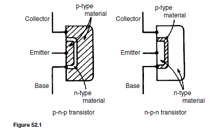
The bipolar junction transistor consists of three regions of semiconductor material. One type is called a p-n-p transistor, in which two regions of p-type material sandwich a very thin layer of n-type material. A second type is called an n-p-n transistor, in which two regions of n-type material sandwich a very thin layer of p-type material. Both of these types of transistors consist of two p-n junctions placed very close to one another in a back-to-back arrangement on a single piece of semiconductor material. Diagrams depicting these two types of transistors are shown in Figure 52.1.

The two p-type material regions of the p-n-p transistor are called the emitter and collector and the n-type material is called the base. Similarly, the two n-type material regions of the n-p-n transistor are called the emitter and collector and the p-type material region is called the base, as shown in Figure 52.1.

Transistors have three connecting leads and in operation an electrical input to one pair of connections, say the emitter and base connections can control the output from another pair, say the collector and emitter connections. This type of operation is achieved by appropriately biasing the two internal p-n junctions. When batteries and resistors are connected to a p-n-p transistor, as shown in Figure 52.2(a), the base-emitter junction is forward biased and the base-collector junction is reverse biased.

Similarly, an n-p-n transistor has its base-emitter junction forward biased and its base-collector junction reverse biased when the batteries are connected as shown in Figure 52.2(b).

For a silicon p-n-p transistor, biased as shown in Figure 52.2(a), if the base-emitter junction is considered on its own, it is forward biased and a

image

image

current flows. This is depicted in Figure 52.3(a). For example, if RE is 1000 Q, the battery is 4.5 V and the voltage drop across the junction is taken as 0.7 V, the current flowing is given by image

When the base-collector junction is considered on its own, as shown in Figure 52.3(b), it is reverse biased and the collector current is something less than 1 µA.

However, when both external circuits are connected to the transistor, most of the 3.8 mA of current flowing in the emitter, which previously flowed from the base connection, now flows out through the collector connection due to transistor action.

Transistor Action

In a p-n-p transistor, connected as shown in Figure 52.2(a), transistor action is accounted for as follows:

(a) The majority carriers in the emitter p-type material are holes

(b) The base-emitter junction is forward biased to the majority carriers and the holes cross the junction and appear in the base region

(c) The base region is very thin and is only lightly doped with electrons so although some electron-hole pairs are formed, many holes are left in the base region

(d) The base-collector junction is reverse biased to electrons in the base region and holes in the collector region, but forward biased to holes in the base region; these holes are attracted by the negative potential at the collector terminal

(e) A large proportion of the holes in the base region cross the base-collector junction into the collector region, creating a collector current; conventional current flow is in the direction of hole movement

The transistor action is shown diagrammatically in Figure 52.4. For transistors having very thin base regions, up to 99.5% of the holes leaving the emitter cross the base collector junction.

In an n-p-n transistor, connected as shown in Figure 52.2(b), transistor action is accounted for as follows:

(a) The majority carriers in the emitter p-type material are electrons

(b) The base-emitter junction is forward biased to these majority carriers and electrons cross the junction and appear in the base region

(c) The base region is very thin and only lightly doped with holes, so some recombination with holes occurs but many electrons are left in the base region

(d) The base-collector junction is reverse biased to holes in the base region and electrons in the collector region, but is forward biased to electrons in the base region; these electrons are attracted by the positive potential at the collector terminal

(e) A large proportion of the electrons in the base region cross the base- collector junction into the collector region, creating a collector current

image

image

The transistor action is shown diagrammatically in Figure 52.5. As stated earlier, conventional current flow is taken to be in the direction of hole flow, that is, in the opposite direction to electron flow, hence the directions of the conventional current flow are as shown in Figure 52.5.

For a p-n-p transistor, the base-collector junction is reverse biased for majority carriers. However, a small leakage current, ICBO flows from the base to the collector due to thermally generated minority carriers (electrons in the collector and holes in the base), being present.

The base-collector junction is forward biased to these minority carriers. If a proportion, ˛, (having a value of up to 0.995 in modern transistors), of the holes passing into the base from the emitter, pass through the base-collector junction, then the various currents flowing in a p-n-p transistor are as shown in Figure 52.6(a).

Similarly, for an n-p-n transistor, the base-collector junction is reversed biased for majority carriers, but a small leakage current, ICBO flows from the collector to the base due to thermally generated minority carriers (holes in the collector and electrons in the base), being present. The base-collector junction is forward biased to these minority carriers. If a proportion, ˛, of the electrons passing through the base-emitter junction also pass through the base-collector junction then the currents flowing in an n-p-n transistor are as shown in Figure 52.6(b).

Transistor Symbols

Symbols are used to represent p-n-p and n-p-n transistors in circuit diagrams and are as shown in Figure 52.7. The arrowhead drawn on the emitter of the symbol is in the direction of conventional emitter current (hole flow). The potentials marked at the collector, base and emitter are typical values for a silicon transistor having a potential difference of 6 V between its collector and its emitter.

The voltage of 0.6 V across the base and emitter is that required to reduce the potential barrier and if it is raised slightly to, say, 0.62 V, it is likely that the collector current will double to about 2 mA. Thus a small change of voltage between the emitter and the base can give a relatively large change of current in the emitter circuit; because of this, transistors can be used as amplifiers.

image

Transistor Connections

There are three ways of connecting a transistor, depending on the use to which it is being put. The ways are classified by the electrode that is common to both the input and the output. They are called:

(a) common-base configuration, shown in Figure 52.8(a)

(b) common-emitter configuration, shown in Figure 52.8(b)

(c) common-collector configuration, shown in Figure 52.8(c)

These configurations are for an n-p-n transistor. The current flows shown are all reversed for a p-n-p transistor.

image

Transistor Characteristics

The effect of changing one or more of the various voltages and currents associated with a transistor circuit can be shown graphically and these graphs are called the characteristics of the transistor. As there are five variables (collector, base and emitter currents, and voltages across the collector and base and emitter and base) and also three configurations, many characteristics are possible. Some of the possible characteristics are given below.

(a) Common-base configuration

(i) Input characteristic. With reference to Figure 52.8(a), the input to a common-base transistor is the emitter current, IE, and can be varied by altering the base emitter voltage VEB . The base-emitter junction is essentially a forward biased junction diode, so as VEB is varied, the current flowing is similar to that for a junction diode, as shown in Figure 52.9 for a silicon transistor. Figure 52.9 is called the input characteristic for an n-p-n transistor having common-base configuration. The variation of the collector-base voltage VCB has little effect on the characteristic. A similar characteristic can be obtained for a p-n-p transistor, these having reversed polarities.

(ii) Output characteristics. The value of the collector current IC is very largely determined by the emitter current, IE. For a given value of IE the collector-base voltage, VCB, can be varied and has little effect on the value of IC. If VCB is made slightly negative, the collector no longer attracts the majority carriers leaving the emitter and IC falls rapidly to zero. A family of curves for various values of IE are possible and some of these are shown in Figure 52.10. Figure 52.10 is called the output characteristics for an n-p-n transistor having common-base configuration. Similar characteristics can be obtained for a p-n-p transistor, these having reversed polarities.

image

image

(b) Common-emitter configuration

(i) Input characteristic. In a common-emitter configuration (see Figure 52.8(b)), the base current is now the input current. As VEB is varied, the characteristic obtained is similar in shape to the input characteristic for a common-base configuration shown in Figure 52.9, but the values of current are far less. With reference to Figure 52.6(a), as long as the junctions are biased as described, the three currents IE, IC and IB keep the ratio I : ˛: (I ð ˛), whichever configuration is adopted. Thus the base current changes are much smaller than the corresponding emitter current changes and the input characteristic for an n-p-n transistor is as shown in Figure 52.11. A similar characteristic can be obtained for a p-n-p transistor, these having reversed polarities.

(ii) Output characteristics. A family of curves can be obtained, depending on the value of base current IB and some of these for an n-p-n transistor are shown in Figure 52.12. A similar set of characteristics can be obtained for a p-n-p transistor, these having reversed polarities. These characteristics differ from the common base output characteristics in two ways:

(a) the collector current reduces to zero without having to reverse the collector voltage, and

(b) the characteristics slope upwards indicating a lower output resistance (usually kilohms for a common-emitter configuration compared with megohms for a common-base configuration).

A circuit diagram for obtaining the input and output characteristics for an n-p-n transistor connected in common-base configuration is shown in Figure 52.13. The input characteristic can be obtained by varying R1, which varies VEB , and noting the corresponding values of IE. This is repeated for various values of VCB. It will be found that the input characteristic is almost independent of VCB and it is usual to give only one characteristic, as shown in Figure 52.9.

image

To obtain the output characteristics, as shown in Figure 52.10, IE is set to a suitable value by adjusting R1. For various values of VCB, set by adjusting R2, IC is noted. This procedure is repeated for various values of IE. To obtain the full characteristics, the polarity of battery V2 has to be reversed to reduce IC to zero. This must be done very carefully or else values of IC will rapidly increase in the reverse direction and burn out the transistor.

The Transistor as an Amplifier

The amplifying properties of a transistor depend upon the fact that current flowing in a low-resistance circuit is transferred to a high-resistance circuit with negligible change in magnitude. If the current then flows through a load resistance, a voltage is developed. This voltage can be many times greater than the input voltage that caused the original current flow.

(a) Common-base amplifier

The basic circuit for a transistor is shown in Figure 52.14 where an n-p- n transistor is biased with batteries b1 and b2 . A sinusoidal alternating input signal, ve, is placed in series with the input bias voltage, and a load resistor, RL ,

image

is placed in series with the collector bias voltage. The input signal is therefore the sinusoidal current ie resulting from the application of the sinusoidal voltage ve superimposed on the direct current IE established by the base-emitter voltage VBE.

Let the signal voltage ve be 100 mV and the base-emitter circuit resistance

image

(b) Common-emitter amplifier

The basic circuit arrangement of a common-emitter amplifier is shown in Figure 52.15. Although two batteries are shown, it is more usual to employ only one to supply all the necessary bias. The input signal is applied between base and emitter, and the load resistor RL is connected between collector and emitter. Let the base bias battery provides a voltage which causes a base current IB of 0.1 mA to flow. This value of base current determines the mean

d.c. level upon which the a.c. input signal will be superimposed. This is the

d.c. base current operating point.

Let the static current gain of the transistor, ˛E, be 50. Since 0.1 mA is the steady base current, the collector current IC will be ˛E ð IB D 50 ð 0.1 D 5 mA. This current will flow through the load resistor RL (D 1 kQ), and there will be a steady voltage drop across RL given by IC RL D 5 ð 10ð3 ð 1000 D 5 V. The voltage at the collector, VCE, will therefore be VCC ð IC RL D 12 ð 5 D 7 V. This value of VCE is the mean (or quiescent) level about which the output signal voltage will swing alternately positive and negative. This is the collector voltage d.c. operating point. Both of these d.c. operating points can be pin-pointed on the input and output characteristics of the transistor. Figure 52.16 shows the IB /VBE characteristic with the operating point X positioned at IB D 0.1 mA, VBE D 0.75 V, say.

Figure 52.17 shows the IC/VCE characteristics, with the operating point Y positioned at IC D 5 mA, VCE D 7 V. It is usual to choose the operating points Y somewhere near the centre of the graph.

image

It is possible to remove the bias battery VBB and obtain base bias from the collector supply battery VCC instead. The simplest way to do this is to connect a bias resistor RB between the positive terminal of the VCC supply and the base as shown in Figure 52.18. The resistor must be of such a value that it allows 0.1 mA to flow in the base-emitter diode.

For a silicon transistor, the voltage drop across the junction for forward bias conditions is about 0.6 V. The voltage across RB must then be 12 – 0.6 =11.4 V. Hence, the value of RB must be such that IB x RB = 11.4 V, i.e. image With the inclusion of the 1 kQ load resistor, RL , a steady 5 mA collector current, and a collector-emitter voltage of 7 V, the d.c. conditions are established.

An alternating input signal (vi) can now be applied. In order not to disturb the bias condition established at the base, the input must be fed to the base by way of a capacitor C1. This will permit the alternating signal to pass to the base but will prevent the passage of direct current. The reactance of this capacitor must be such that it is very small compared with the input resistance of the transistor. The circuit of the amplifier is now as shown in Figure 52.19. The a.c. conditions can now be determined.

When an alternating signal voltage v1 is applied to the base via capacitor C1 the base current ib varies. When the input signal swings positive, the base current increases; when the signal swings negative, the base current decreases. The base current consists of two components: IB , the static base bias established by RB , and ib , the signal current. The current variation ib will in turn vary the collector current, iC . The relationship between iC and ib is given by

image

iC = ˛e ib , where ˛e is the dynamic current gain of the transistor and is not quite the same as the static current gain ˛E; the difference is usually small enough to be insignificant.

The current through the load resistor RL also consists of two components: IC, the static collector current, and iC, the signal current. As ib increases, so does iC and so does the voltage drop across RL . Hence, from the circuit:

image

The d.c. components of this equation, though necessary for the amplifier to operate at all, need not be considered when the a.c. signal conditions are being examined. Hence, the signal voltage variation relationship is:

image

the negative sign being added because vce decreases when ib increases and vice versa. The signal output and input voltages are of opposite polarity i.e.

a phase shift of 180° has occurred. So that the collector d.c. potential is not passed on to the following stage, a second capacitor, C2 , is added as shown in Figure 52.19. This removes the direct component but permits the signal voltage vo = iC RL to pass to the output terminals.

The Load Line

The relationship between the collector-emitter voltage (VCE) and collector current (IC) is given by the equation: VCE = VCC – ICRL in terms of the d.c. conditions. Since VCC and RL are constant in any given circuit, this represents the equation of a straight line which can be written in the y D mx C c form. Transposing VCE = VCC – ICRL for IC gives:

image

A family of collector static characteristics drawn on such axes is shown in Figure 52.12 on page 318, and so the line may be superimposed on these as shown in Figure 52.20.

The reason why this line is necessary is because the static curves relate IC to VCE for a series of fixed values of IB . When a signal is applied to the base of the transistor, the base current varies and can instantaneously take any of the values between the extremes shown. Only two points are necessary to draw the line and these can be found conveniently by considering extreme

image

Thus the points A and B respectively are located on the axes of the IC/VCE characteristics. This line is called the load line and it is dependent for its position upon the value of VCC and for its gradient upon RL . As the gradient is given by  image , the slope of the line is negative.

For every value assigned to RL in a particular circuit there will be a corresponding (and different) load line. If VCC is maintained constant, all the possible lines will start at the same point (B) but will cut the IC axis at different points A. Increasing RL will reduce the gradient of the line and vice-versa. Quite clearly the collector voltage can never exceed VCC (point B) and equally the collector current can never be greater than that value which would make VCE zero (point A).

Using the circuit example of Figure 52.15, we have

image

The load line is drawn on the characteristics shown in Figure 52.21, which we assume are characteristics for the transistor used in the circuit of Figure 52.15 earlier. Notice that the load line passes through the operating point X, as it should, since every position on the line represents a relationship between VCE and IC for the particular values of VCC and RL given. Suppose

image

that the base current is caused to vary š0.1 mA about the d.c. base bias of 0.1 mA. The result is IB changes from 0 mA to 0.2 mA and back again to 0 mA during the course of each input cycle. Hence the operating point moves up and down the load line in phase with the input current and hence the input voltage. A sinusoidal input cycle is shown on Figure 52.21.

Current and Voltage Gains

The output signal voltage (vce) and current (iC) can be obtained by projecting vertically from the load line on to VCE and IC axes respectively. When the input current ib varies sinusoidally as shown in Figure 52.21, then vce varies sinusoidally if the points E and F at the extremities of the input variations are equally spaced on either side of X.

The peak to peak output voltage is seen to be 8.5 V, giving an r.m.s. value of image The peak-to-peak output current is 8.75 mA, 2 giving an r.m.s. value of 3.1 mA. From these figures the voltage and current amplifications can be obtained.

The dynamic current gain Ai (D˛e ) as opposed to the static gain ˛E, is given by:

image

This always leads to a different figure from that obtained by the direct division of image which assumes that the collector load resistor is zero. From Figure 52.21 the peak input current is 0.1 mA and the peak output current is

image

This cannot be calculated from the data available, but if we assume that the base current flows in the input resistance, then the base voltage can be determined. The input resistance can be determined from an input characteristic such as was shown earlier.

image

Thermal Runaway

When a transistor is used as an amplifier it is necessary to ensure that it does not overheat. Overheating can arise from causes outside of the transistor itself, such as the proximity of radiators or hot resistors, or within the transistor as the result of dissipation by the passage of current through it. Power dissipated within the transistor, which is given approximately by the product IC VCE, is wasted power; it contributes nothing to the signal output power and merely raises the temperature of the transistor. Such overheating can lead to very undesirable results.

The increase in the temperature of a transistor will give rise to the production of hole electron pairs, hence an increase in leakage current represented by the additional minority carriers. In turn, this leakage current leads to an increase in collector current and this increases the product IC VCE. The whole effect thus becomes self-perpetuating and results in thermal runaway. This rapidly leads to the destruction of the transistor.

Two basic methods of preventing thermal runaway are available and either or both may be used in a particular application:

Method 1. The use of a single biasing resistor RB as shown earlier in Figure 52.18 is not particularly good practice. If the temperature of the transistor increases, the leakage current also increases. The collector current, collector voltage and base current are thereby changed, the base current decreasing as

image

IC increases. An alternative is shown in Figure 52.22. Here the resistor RB is returned, not to the VCC line, but to the collector itself.

If the collector current increases for any reason, the collector voltage VCE will fall. Therefore, the d.c. base current IB will fall, since image . Hence the collector current IC D ˛EIB will also fall and compensate for the original increase.

A commonly used bias arrangement is shown in Figure 52.23. If the total resistance value of resistors R1 and R2 is such that the current flowing through the divider is large compared with the d.c. bias current IB , then the base voltage VBE will remain substantially constant regardless of variations in collector current. The emitter resistor RE in turn determines the value of emitter current which flows for a given base voltage at the junction of R1 and R2. Any increase in IC produces an increase in IE and a corresponding increase in the voltage drop across RE. This reduces the forward bias voltage VBE and leads to a compensating reduction in IC

Method 2. This method concerns some means of keeping the transistor temperature down by external cooling. For this purpose, a heat sink is employed, as shown in Figure 52.24 If the transistor is clipped or bolted to a large conducting area of aluminium or copper plate (which may have cooling fins), cooling is achieved by convection and radiation.

Heat sinks are usually blackened to assist radiation and are normally used where large power dissipation’s are involved. With small transistors, heat sinks are unnecessary. Silicon transistors particularly have such small leakage cur- rents that thermal problems rarely arise.


image


Electrical Measuring Instruments and Measurements

Introduction

Tests and measurements are important in designing, evaluating, maintaining and servicing electrical circuits and equipment. In order to detect electrical quantities such as current, voltage, resistance or power, it is necessary to transform an electrical quantity or condition into a visible indication. This is done with the aid of instruments (or meters) that indicate the magnitude of quantities either by the position of a pointer moving over a graduated scale (called an analogue instrument) or in the form of a decimal number (called a digital instrument).

Analogue Instruments

All analogue electrical indicating instruments require three essential devices:

(a) A deflecting or operating device. A mechanical force is produced by the current or voltage which causes the pointer to deflect from its zero position.

(b) A controlling device. The controlling force acts in opposition to the deflecting force and ensures that the deflection shown on the meter is always the same for a given measured quantity. It also prevents the pointer always going to the maximum deflection. There are two main types of controlling device — spring control and gravity control.

(c) A damping device. The damping force ensures that the pointer comes to rest in its final position quickly and without undue oscillation. There are

three main types of damping used — eddy-current damping, air-friction damping and fluid-friction damping.

There are basically two types of scale — linear and non-linear.

A linear scale is shown in Figure 50.1(a), where the divisions or grad- uations are evenly spaced. The voltmeter shown has a range 0– 100 V, i.e. a full-scale deflection (f.s.d.) of 100 V. A non-linear scale is shown in Figure 50.1(b) where the scale is cramped at the beginning and the graduations are uneven throughout the range. The ammeter shown has a f.s.d. of 10 A.

image

Moving-iron Instrument

(a) An attraction type of moving-iron instrument is shown diagrammatically in Figure 50.2(a). When current flows in the solenoid, a pivoted soft-iron disc is attracted towards the solenoid and the movement causes a pointer to move across a scale.

(b) In the repulsion type moving-iron instrument shown diagrammatically in Figure 50.2(b), two pieces of iron are placed inside the solenoid, one being fixed, and the other attached to the spindle carrying the pointer. When current passes through the solenoid, the two pieces of iron are magnetised in the same direction and therefore repel each other. The pointer thus moves across the scale. The force moving the pointer is, in each type, proportional to I2 and because of this the direction of current does not matter. The moving-iron instrument can be used on d.c. or a.c.; the scale, however, is non-linear.

image

The Moving-coil Rectifier Instrument

A moving-coil instrument, which measures only d.c., may be used in con- junction with a bridge rectifier circuit as shown in Figure 50.3 to provide an indication of alternating currents and voltages (see chapter 54). The aver- age value of the full wave rectified current is 0.637 Im . However, a meter being used to measure a.c. is usually calibrated in r.m.s. values. For sinusoidal image times the mean value. Rectifier instruments have scales calibrated in r.m.s. quantities and it is assumed by the manufacturer that the a.c. is sinusoidal.

image

image

Shunts and Multipliers

An ammeter, which measures current, has a low resistance (ideally zero) and must be connected in series with the circuit.

A voltmeter, which measures p.d., has a high resistance (ideally infinite) and must be connected in parallel with the part of the circuit whose p.d. is required.

There is no difference between the basic instrument used to measure current and voltage since both use a milliammeter as their basic part. This is a sensitive instrument that gives f.s.d. for currents of only a few milliamperes. When an ammeter is required to measure currents of larger magnitude, a pro- portion of the current is diverted through a low-value resistance connected in parallel with the meter. Such a diverting resistor is called a shunt.

image

image

Electronic Instruments

Electronic measuring instruments have advantages over instruments such as the moving-iron or moving-coil meters, in that they have a much higher input resistance (some as high as 1000 Mˇ) and can handle a much wider range of frequency (from d.c. up to MHz).

The digital voltmeter (DVM) is one that provides a digital display of the voltage being measured. Advantages of a DVM over analogue instruments include higher accuracy and resolution, no observational or parallex errors (see later) and a very high input resistance, constant on all ranges.

A digital multimeter is a DVM with additional circuitry that makes it capable of measuring a.c. voltage, d.c. and a.c. current and resistance.

Instruments for a.c. measurements are generally calibrated with a sinusoidal alternating waveform to indicate r.m.s. values when a sinusoidal signal is applied to the instrument. Some instruments, such as the moving-iron and electro-dynamic instruments, give a true r.m.s. indication. With other instruments the indication is either scaled up from the mean value (such as with the rectified moving-coil instrument) or scaled down from the peak value.

Sometimes quantities to be measured have complex waveforms (see chapter 76), and whenever a quantity is non-sinusoidal, errors in instrument readings can occur if the instrument has been calibrated for sine waves only. Using electronic instruments can largely eliminate such waveform errors.

The Ohmmeter

An ohmmeter is an instrument for measuring electrical resistance. A simple ohmmeter circuit is shown in Figure 50.5(a). Unlike the ammeter or voltmeter, the ohmmeter circuit does not receive the energy necessary for its operation from the circuit under test. In the ohmmeter this energy is supplied by a self-contained source of voltage, such as a battery. Initially, terminals XX are short-circuited and R adjusted to give f.s.d. on the milliammeter. If current I is at a maximum value and voltage E is constant, then resistance R D E/I is at a minimum value. Thus f.s.d. on the milliammeter is made zero on the resistance scale. When terminals XX are open circuited no current flows and R(D E/O) is infinity

image

The milliammeter can thus be calibrated directly in ohms. A cramped (non-linear) scale results and is ‘back to front’, as shown in Figure 50.5(b). When calibrated, an unknown resistance is placed between terminals XX and its value determined from the position of the pointer on the scale. An ohmmeter designed for measuring low values of resistance is called a continuity tester. An ohmmeter designed for measuring high values of resistance (i.e. megohms) is called an insulation resistance tester (e.g. ‘Megger’)

Multimeters

Instruments are manufactured that combine a moving-coil meter with a number of shunts and series multipliers, to provide a range of readings on a single scale graduated to read current and voltage. If a battery is incorporated then resistance can also be measured. Such instruments are called multimeters or universal instruments or multirange instruments. An ‘Avometer’ is a typical example. A particular range may be selected either by the use of separate terminals or by a selector switch. Only one measurement can be performed at a time. Often such instruments can be used in a.c. as well as d.c. circuits when a rectifier is incorporated in the instrument.

Wattmeters

A wattmeter is an instrument for measuring electrical power in a circuit. Figure 50.6 shows typical connections of a wattmeter used for measuring power supplied to a load. The instrument has two coils:

image

(i) a current coil, which is connected in series with the load, like an ammeter, and

(ii) a voltage coil, which is connected in parallel with the load, like a volt- meter.

Instrument ‘Loading’ Effect

Some measuring instruments depend for their operation on power taken from the circuit in which measurements are being made. Depending on the ‘loading’ effect of the instrument (i.e. the current taken to enable it to operate), the prevailing circuit conditions may change.

The resistance of voltmeters may be calculated since each have a stated sensitivity (or ‘figure of merit’), often stated in ‘kˇ per volt’ of f.s.d. A voltmeter should have as high a resistance as possible (- ideally infinite). In a.c. circuits the impedance of the instrument varies with frequency and thus the loading effect of the instrument can change.

The Cathode Ray Oscilloscope

The cathode ray oscilloscope (c.r.o.) may be used in the observation of waveforms and for the measurement of voltage, current, frequency, phase and periodic time. For examining periodic waveforms the electron beam is deflected horizontally (i.e. in the X direction) by a sawtooth generator acting as a timebase. The signal to be examined is applied to the vertical deflection system (Y direction) usually after amplification.

Oscilloscopes normally have a transparent grid of 10 mm by 10 mm squares in front of the screen, called a graticule. Among the timebase controls is a ‘variable’ switch that gives the sweep speed as time per centimetre. This may be in s/cm, ms/cm or µs/cm, a large number of switch positions being available. Also on the front panel of a c.r.o. is a Y amplifier switch marked in volts per centimetre, with a large number of available switch positions.

(i) With direct voltage measurements, only the Y amplifier ‘volts/cm’ switch on the c.r.o. is used. With no voltage applied to the Y plates the position of the spot trace on the screen is noted. When a direct voltage is applied to the Y plates the new position of the spot trace is an indication of the magnitude of the voltage. For example, in Figure 50.7(a), with no voltage applied to the Y plates, the spot trace is in the centre of the screen (initial position) and then the spot trace moves 2.5 cm to the final position shown, on application of a d.c. voltage. With the ‘volts/cm’ switch on 10 volts/cm the magnitude of the direct voltage is 2.5 cm ð 10 volts/cm, i.e. 25 volts.

(ii) With alternating voltage measurements, let a sinusoidal waveform be displayed on a c.r.o. screen as shown in Figure 50.7(b). If the time/cm switch is on, say, 5 ms/cm then the periodic time T of the sinewave is 5 ms/cm ð 4 cm, i.e. 20 ms or 0.02 s

image

image

Double beam oscilloscopes are useful whenever two signals are to be compared simultaneously.

For example, for the double-beam oscilloscope displays shown in Figure 50.8, the ‘time/cm’ switch is on 100 µs/cm and the ‘volts/cm’ switch on 2 V/cm. The width of each complete cycle is 5 cm for both waveforms.

Hence the periodic time, T, of each waveform is 5 cm ð 100 µs/cm =0.5 ms

image

The c.r.o. demands reasonable skill in adjustment and use. However its greatest advantage is in observing the shape of a waveform — a feature not possessed by other measuring instruments.

Logarithmic Ratios

In electronic systems, the ratio of two similar quantities measured at different points in the system, are often expressed in logarithmic units. By definition, if the ratio of two powers P1 and P2 is to be expressed in decibel (dB) units then the number of decibels, X, is given by:

image

For example, an amplifier has a gain of 14 dB and its input power is 8 mW. Its output power is determined as follows:

image

Logarithmic units may also be used for voltage and current ratios. The number of decibels, X, is given by:

image

From equation (1), X decibels is a logarithmic ratio of two similar quantities and is not an absolute unit of measurement. It is therefore necessary to state a reference level to measure a number of decibels above or below that reference. The most widely used reference level for power is 1 mW, and when power levels are expressed in decibels, above or below the 1 mW reference level, the unit given to the new power level is dBm.

A voltmeter can be re-scaled to indicate the power level directly in decibels. The scale is generally calibrated by taking a reference level of 0 dB

when a power of 1 mW is dissipated in a 600 ˇ resistor (this being the natural impedance of a simple transmission line). The reference voltage V is then

image

Null Method of Measurement

A null method of measurement is a simple, accurate and widely used method which depends on an instrument reading being adjusted to read zero current only. The method assumes:

(i) if there is any deflection at all, then some current is flowing

(ii) if there is no deflection, then no current flows (i.e. a null condition).

Hence it is unnecessary for a meter sensing current flow to be calibrated when used in this way. A sensitive milliammeter or microammeter with centre zero position setting is called a galvanometer. Examples where the method is used are in the Wheatstone bridge, in the d.c. potentiometer and with a.c. bridges (see chapter 67)

Wheatstone Bridge

Figure 50.10 shows a Wheatstone bridge circuit that compares an unknown resistance Rx with others of known values, i.e. R1 and R2, which have fixed values, and R3, which is variable. R3 is varied until zero deflection is obtained on the galvanometer G. No current then flows through the meter, VA D VB , and the bridge is said to be ‘balanced’

image

D.c. Potentiometer

The d.c. potentiometer is a null-balance instrument used for determining values of e.m.f.’s and p.d.s. by comparison with a known e.m.f. or p.d. In Figure 50.11(a), using a standard cell of known e.m.f. E1, the slider S is moved along the slide wire until balance is obtained (i.e. the galvanometer deflection is zero), shown as length l1

The standard cell is now replaced by a cell of unknown e.m.f. E2 (see Figure 50.11(b)) and again balance is obtained (shown as l2).

image

A potentiometer may be arranged as a resistive two-element potential divider in which the division ratio is adjustable to give a simple variable d.c. supply. Such devices may be constructed in the form of a resistive element carrying a sliding contact that is adjusted by a rotary or linear movement of the control knob.

image

Q-meter

The Q-factor for a series L-C-R circuit is the voltage magnification at resonance, i.e. image

The simplified circuit of a Q-meter, used for measuring Q-factor, is shown in Figure 50.12. Current from a variable frequency oscillator flowing through a very low resistance r develops a variable frequency voltage, Vr , which is applied to a series L-R-C circuit. The frequency is then varied until resonance causes voltage Vc to reach a maximum value. At resonance Vr and Vc are noted.

image

In a practical Q-meter, Vr is maintained constant and the electronic volt- meter can be calibrated to indicate the Q-factor directly. If a variable capacitor C is used and the oscillator is set to a given frequency, then C can be adjusted to give resonance. In this way inductance L may be calculated using

image

Q-meters operate at various frequencies and instruments exist with frequency ranges from 1 kHz to 50 MHz. Errors in measurement can exist with Q-meters since the coil has an effective parallel self-capacitance due to capacitance between turns. The accuracy of a Q-meter is approximately +-5%.

Measurement Errors

Errors are always introduced when using instruments to measure electrical quantities. The errors most likely to occur in measurements are those due to:

(i) the limitations of the instrument

(ii) the operator

(iii) the instrument disturbing the circuit

(i) Errors in the limitations of the instrument

The calibration accuracy of an instrument depends on the precision with which it is constructed. Every instrument has a margin of error that is expressed as a percentage of the instruments full scale deflection. For example, industrial grade instruments have an accuracy of š2% of f.s.d. Thus if a voltmeter has a f.s.d. of 100 V and it indicates 40 V say, then the actual voltage may be anywhere between 40 š (2% of 100), or 40 š 2, i.e. between 38 V and 42 V. When an instrument is calibrated, it is compared against a standard instrument and a graph is drawn of ‘error’ against ‘meter deflection’. A typical graph is shown in Figure 50.13 where it is seen that the accuracy varies over the scale length. Thus, a meter with a š2% f.s.d. accuracy would tend to have an accuracy which is much better than š2% f.s.d. over much of the range.

image

(ii) Errors by the operator

It is easy for an operator to misread an instrument. With linear scales the values of the sub-divisions are reasonably easy to determine; non-linear scale graduations are more difficult to estimate. Also, scales differ from instrument to instrument and some meters have more than one scale (as with multimeters) and mistakes in reading indications are easily made. When reading a meter scale it should be viewed from an angle perpendicular to the surface of the scale at the location of the pointer; a meter scale should not be viewed ‘at an angle’.

(iii) Errors due to the instrument disturbing the circuit

Any instrument connected into a circuit will affect that circuit to some extent. Meters require some power to operate, but provided this power is small com- pared with the power in the measured circuit, then little error will result. Incorrect positioning of instruments in a circuit can be a source of errors. For example, let a resistance be measured by the voltmeter-ammeter method as shown in Figure 50.14. Assuming ‘perfect’ instruments, the resistance should be given by the voltmeter reading divided by the ammeter reading (i.e. R D V/I). However, in Figure 50.14(a), V/I D R C ra and in Figure 50.14(b) the current through the ammeter is that through the resistor plus that through the voltmeter. Hence the voltmeter reading divided by the ammeter reading will not give the true value of the resistance R for either method of connection.

image