SMES Circuit and Control Techniques
3.1 Principle and Operation Theory
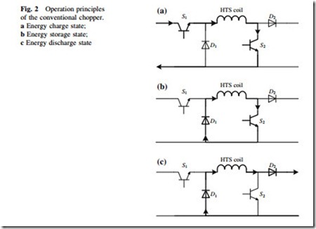
In general, the SMES-based power apparatuses have the dynamic electric energy exchange between a superconducting coil and an external interface for a power system. With regard to the SMES control, a conventional chopper having two power switches and two power diodes is mostly applied to link the HTS coil to the DC bus and to achieve the bidirectional power exchange for managing the generated power of distributed generators (DGs) or maintaining the uninterruptible power of critical electric equipment. As shown in Fig. 1, a typical power conditioning system (PCS) with voltage source converter (VSC), it has three main operation states, i.e., energy charge state, energy storage state, and energy dis- charge state. The HTS coil is charged by a DC power source through the power switches S1, S2, then stores its magnetic energy through the power switch S2 and the power diode D1, and finally discharges its stored energy to the external load through the power diodes D1 and D2, respectively. Figure 2 shows the operation principles of the conventional chopper.
According to the state-of-the-art power electronic technologies [12], the appli- cable voltage rating of the insulated gate bipolar translators (IGBTs) is between 0.5 and 6.5 kV. Since the most SMES devices currently are developed for low voltage power distribution applications [13], having operation voltages across the HTS coils at kV level, IGBTs are normally applied to form a conventional chopper. Even when the operation voltage across the HTS coils drops to 750 V in the ongoing 2.4 GJ SMES project [14], IGBTs still have the advantages over MOSFETs.
However, if the applicable voltage ratings are below 500 V, the metal oxide semiconductor field effect transistors (MOSFETs) are more suitable to achieve high-efficiency and high power energy conversions for various end-users’ applications such as EVs [15] and UPSs [16]. Meanwhile, the turn-on resistances in the commercial low-voltage MOSFETs have already been reduced to Milliohm level or below, which results in much lower consumed power than that in the power diodes.
Recently, new focuses of low-voltage SMES applications have been formed for various power end-users. The rapid developments of hydrogen-powered fuel cell vehicles (FCVs) make it available to cool the HTS or MgB2 coils by fully making use of the onboard liquid hydrogen (LH2). The SMES technology has been technically verified [17, 18] to improve the fast repeated charge–discharge performance for regenerative braking. Meanwhile, some low-voltage direct-current (LVDC) power transmission systems have been proposed and studied to connect with various DC output type distributed generators (DGs) [19] such as photovoltaic (PV) cells and fuel cells (FCs), and to supply the electric loads in the commercial and
residential buildings [20]. The superconducting DC cable with nearly zero energy loss has been applied to achieve high power and long-distance power transmission, with an additional SMES device introduced to enhance the whole power transfer capacity and stability [21, 22]. In the above low-voltage applications, several considerable benefits from the SMES technology can be derived to improve the power quality for the end-user, to achieve high-efficiency operation for energy saving, and to lower the capital cost of the SMES device. Therefore, beside the current large-scale SMES applications for power transmission and distribution, small-scale SMES devices also have very promising application prospects for use in the power end-user systems.
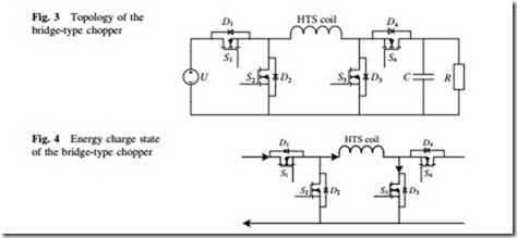
Consequently, a new bridge-type chopper using MOSFETs is proposed [23] and analyzed to reduce the energy loss for low-voltage applications. The circuit topology of the bridge-type chopper is shown in Fig. 3. It mainly consists of four low-loss power electronic switches, i.e., MOSFETs S1–S4 paralleled with their reverse diodes D1–D4, and a DC-link capacitor C paralleled to the load R. Like the conventional chopper, it also has the same three main operation states. In addition, owning to the inevitable turn-on and turn-off delayed time of a practical power switch, two transient operation states are necessary to avoid potential short circuits of the DC power supply and DC-link capacitor.
When the bridge-type chopper operates at energy charge state, the HTS coil L is charged by a DC power supply U through S1 and S3, as shown in Fig. 4. The circuit voltage equation can be expressed by
where IL(t), transient current through the HTS coil; RL, lossy resistance from the connection junctions and current leads in the HTS coil; Rs, turn-on resistance of the MOSFET unit.
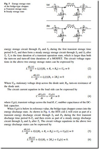
When IL(t) reaches its reference value, the bridge-type chopper comes into the energy storage state. As shown in Fig. 5, the HTS coil L will form a transient Fig. 5 Energy storage state of the bridge-type chopper. a Transient storage state;
Principle of Control and Protection
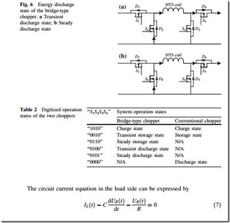
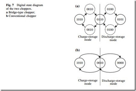
Defining the turn-on or turn-off status of a power switch as ‘‘1’’ or ‘‘0’’, the system operation states of the bridge-type and conventional choppers can be digitalized, as shown in Table 2. Besides the three steady operation states of charge state, storage state, and discharge state in the conventional chopper, the bridge-type one has two more transient operation states to avoid the short circuits of the power source and DC-link capacitor, as shown in Fig. 7. In practice, the HTS coil is normally controlled to carry out the bidirectional energy exchanges with the external sys- tem. A digital control method is consequently introduced to achieve the controlled energy charge, storage, and discharge processes. In normal operation, when the load resistor is operated at a power swell state, the real-time operation state of the
two choppers will be converted between charge state and storage state alternately to absorb the surplus power. Similarly, when the load resistor is operated at a power sag state, the real-time operation state will be converted between discharge state and storage state alternately to compensate the shortfall power. The above two dynamic processes can be defined as ‘‘charge-storage mode’’ and ‘‘discharge- storage mode’’.
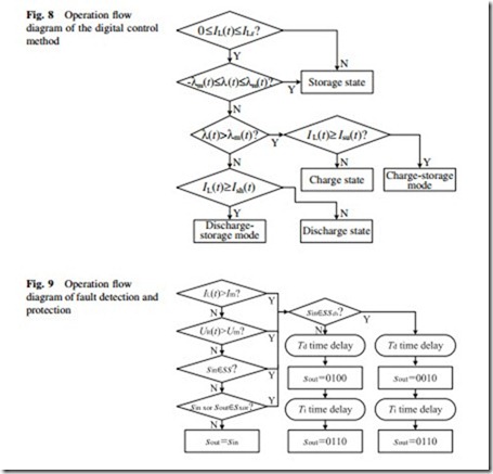
A concept of maximum permissible relative voltage error km(t) is introduced to divide the three main operation states, and can be expressed by
where Umax(t) and Ur(t) are the maximum overshoot voltage and rated voltage across the DC-link capacitor and resistive load; Ur is reference voltage.
Thus the three main operation states are described as follows: (i) When the instantaneous relative voltage error k(t) meets the condition of -km(t) B k(t) B km(t), the chopper is operated at energy storage state; (ii) When k(t) meets the condition of k(t) \ -km(t), the chopper is operated at energy dis- charge state; (iii) When k(t) meets the condition of k(t) [ km(t), the chopper is operated at energy charge state. During the dynamic energy exchange processes, the chopper will be operated at a charge-storage mode or a discharge-storage mode when IL(t) is larger than the shortfall current Ish(t) or surplus current Isu(t). ILr is the rated current through the HTS coil. The whole operation flow diagram of the digital control method developed is shown in Fig. 8.
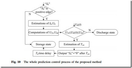
In addition, a fault detection and protection module is particularly required to avoid the potential risks like short circuit, overcurrent, and overvoltage. Four main fault operations are described as follows: (i) IL(t) exceeds its maximum allowable value Im; (ii) UR(t) exceeds its maximum allowable value Um; (iii) The current input signals sin of the module do not belong to the sequences ss of all the digital control signals in Fig. 7; (iv) The value of sin xor sout does not belong to the sequences sxor of ‘‘0001’’, ‘‘0010’’, ‘‘0100’’, and ‘‘1000’’. If a fault operation is detected, the current operation state should be converted into storage state immediately, as shown in Fig. 9. sout is the last output signals of the module. ssch is the sequences of the digital control signals in the charge-storage mode. Td is an inevitable time delay in a practical digital control system.
Principle and Implementation of a Novel Digital Prediction Control Method To achieve high-performance applications and avoid operation risks caused by various real-time statuses such as critical current, AC loss, and electromagnetic force, superconducting magnets generally need to operate precisely during the charge, storage, and discharge processes. However, owning to the existence of an inevitable time delay consisting of the sampling time of the controlled variables, computing time of the digital control chip, and implementing time of the con- trolled objects [24, 25], the digital control signals from a practical digital system usually lag behind the changes of the controlled variables, which results in some undesired overshoots.
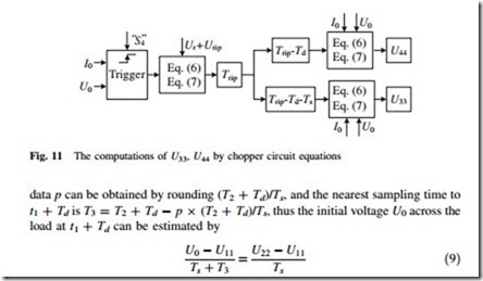
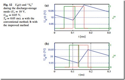
A new digital prediction control method is proposed to limit the controlled variables into their desired reference ripple ranges. The principle is to predict the instantaneous time tr when the practical controlled variable, e.g., UR(t), reaches its reference value and to output the corresponding digital control signals at tr – Td in advance. The whole prediction control process during the discharge-storage mode is shown in Fig. 10 and particularly presented as follows.
The Estimations of the Initial Current and Voltage Values by Linear Extrapolation Method Assume that the digital control chip outputs the state-switching signals at a certain time t1, and the time interval from the nearest sampling time to t1 is T2, thus the bridge-type chopper will change its operation state at t1 ? Td. However, IL(t) and UR(t) at t1 ? Td are very difficult to be sampled precisely because the practical sampling time period Ts cannot be infinitely small. The number of the sampled
where U11 and U22 are the sampled voltage values at T3 – Ts and T3, respectively. The initial current I0 through the superconducting magnet at t1 ? Td can be estimated by the similar method.
The Computations of the Critical Voltage Values by Chopper Circuit Equations Applying the estimated initial current and voltage values (I0, U0) into (6) and (7), UR(t) during the current operation state can be computed and predicted. Assume that the permissible voltage ripple range is from Ur – Urip to Ur ? Urip, thus the time Trip, when UR(t) = Ur ? Urip, can be computed by (6) and (7) in the energy discharge state, and the digital control chip should output the state-switching signals at Trip – Td. As shown in Fig. 11, UR(t) at Trip – Td – Ts and Trip – Td are computed and defined as two critical voltage values (U33, U44) for state-switching judgement.
The Estimation of the State-Switching Time by Linear Interpolation Method The sampled UR(t) is used to compare with U33 and U44, and to predict the precise state-switching time. When U33 B UR(t) B U44, the time interval Tsw from the sampled time to Trip – Td can be estimated by
Thus the digital control chip outputs the state-switching signals after Tsw, and finally makes the bridge-type chopper convert into storage state when UR(t) = Ur ? Urip.
Figure 12 shows the voltage curve (blue line) across the external load and its corresponding digital control signal ‘‘S4’’ for the switch S4 by using the conventional and improved methods. If the turn-on and turn-off time delay of a switch is ignored, the practical state-switching control signal (red dotted line) corresponds to the voltage overshoots. However, if the improved method is applied, the digital control chip will output the state-switching control signal (green line) 0.05 ms before the time when UR(t) reaches 9.95 or 10.05 V, thus UR(t) can be precisely limited from 9.95 to 10.05 V.
