Noise Levels
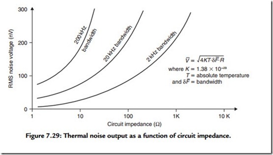
Improved manufacturing techniques have lessened the differences between the various types of semiconductor devices in respect to intrinsic noise level. For most practical purposes it can now be assumed that the characteristics of the device will be defined by the thermal noise figure of the circuit impedances. This relationship is shown in the graph of Figure 7.29.
For very low noise systems, operating at circuit impedance levels that have been deliberately chosen to be as low as practicable—such as in moving coil PU head amplifiers—bipolar junction transistors are still the preferred device. These will either be chosen to have a large base junction area or will be employed as a parallel-connected array, as, for example, in the LM194/394 “super-match pair” ICs, where a multiplicity of parallel-connected transistors are fabricated on a single chip, giving an effective input (noise) impedance as low as 40 ohms.
However, recent designs of monolithic-dual J-FETs, using a similar type of multiple parallel-connection system, such as the Hitachi 2SK389, can offer equivalent thermal noise resistance values as low as 33 ohms and a superior overall noise figure at input resistance values in excess of 100 ohms.
At impedance levels beyond about 1 kilohm there is little practical difference between any devices of recent design. Earlier MOSFET types were not so satisfactory because of excess noise effects arising from carrier-trapping mechanisms in impurities at the channel/gate interface.
