A circuit designed to convert a low voltage to a higher voltage is called a voltage amplifier. A circuit designed to convert a low current to a higher current is called a current amplifier.
Amplifier Configurations
In order for a transistor to provide amplification, it must be able to accept an input signal and produce an output signal that is greater than the input.
The input signal controls current flow in the transistor. This in turn controls the voltage through the load. The transistor circuit is designed to take voltage from an external power source (VCC) and apply it to a load resistor (RL) in the form of an output voltage. The output voltage is controlled by a small input voltage.
The transistor is used primarily as an amplifying device. However, there is more than one way of achieving this amplification. The transistor can be connected in three different circuit configurations.
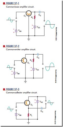
The three circuit configurations are the common- base circuit, the common-emitter circuit, and the common-collector circuit. In each configuration, one of the transistor’s leads serves as a common reference point, and the other two leads serve as input and output connections. Each configuration can be constructed using either NPN or PNP transistors. In each, the transistor’s emitter-base junction is forward biased, whereas the collector-base junction is reverse biased. Each configuration offers advantages and disadvantages.
In the common-base circuit (Figure 37-1), the input signal enters the emitter-base circuit, and the output leaves from the collector-base circuit. The base is the element common to both the input and output circuits.
In the common-emitter circuit (Figure 37-2), the input signal enters the base-emitter circuit, and the output signal leaves from the collector-emitter circuit. The emitter is common to both the input and output circuits. This method of connecting a transistor is the most widely used.
The third type of connection (Figure 37-3) is the common-collector circuit. In this configuration, the input signal enters the base-collector circuit, and the output signal leaves from the emitter-collector circuit. Here, the collector is common to both the
input and output circuits. This circuit is used as an impedance-matching circuit.
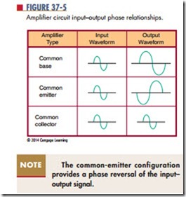
Figure 37-4 charts the input–output resistance and the voltage, current, and power gains for the three circuit configurations. Figure 37-5 shows the phase relationship of input and output waveforms for the three configurations.
Questions
1. Draw schematic diagrams of the three basic configurations of transistor amplifier circuits.
2. List the characteristics of the following circuit configurations:
a. Common-base circuit
b. Common-emitter circuit
c. Common-collector circuit
3. Make a chart showing the input–output phase
4. Make a chart showing the input–output resistances of the three configurations.
5.Make a chart showing the voltage, current, and power gains of the three configurations


